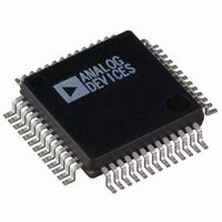
ADUC842BSZ62-5 Analog Devices Inc, ADUC842BSZ62-5 Datasheet - Page 36

ADUC842BSZ62-5
Manufacturer Part Number
ADUC842BSZ62-5
Description
IC ADC/DAC 12BIT W/MCU 52-MQFP
Manufacturer
Analog Devices Inc
Series
MicroConverter® ADuC8xxr
Specifications of ADUC842BSZ62-5
Core Size
8-Bit
Program Memory Size
62KB (62K x 8)
Oscillator Type
Internal
Core Processor
8052
Speed
16.78MHz
Connectivity
I²C, SPI, UART/USART
Peripherals
DMA, PSM, PWM, Temp Sensor, WDT
Number Of I /o
32
Program Memory Type
FLASH
Ram Size
2.25K x 8
Voltage - Supply (vcc/vdd)
4.75 V ~ 5.25 V
Data Converters
A/D 8x12b, D/A 2x12b
Operating Temperature
-40°C ~ 85°C
Package / Case
52-MQFP, 52-PQFP
Controller Family/series
(8052) ADUC
No. Of I/o's
34
Ram Memory Size
2KB
Cpu Speed
16.78MHz
No. Of Timers
3
No. Of Pwm
RoHS Compliant
Lead Free Status / RoHS Status
Lead free / RoHS Compliant
Eeprom Size
-
Lead Free Status / RoHS Status
Lead free / RoHS Compliant
Available stocks
Company
Part Number
Manufacturer
Quantity
Price
Company:
Part Number:
ADUC842BSZ62-5
Manufacturer:
Analog Devices Inc
Quantity:
10 000
Part Number:
ADUC842BSZ62-5
Manufacturer:
ADI/亚德诺
Quantity:
20 000
ADuC841/ADuC842/ADuC843
ADuC842/ADuC843 Configuration SFR (CFG842)
The CFG842 SFR contains the necessary bits to configure the
internal XRAM, external clock select, PWM output selection,
DAC buffer, and the extended SP for both the ADuC842 and the
ADuC843. By default, it configures the user into 8051 mode, i.e.,
extended SP is disabled and internal XRAM is disabled. On the
ADuC841, this register is the CFG841 register and is described
on the next page.
Table 13. CFG842 SFR Bit Designations
Bit No.
7
6
5
4
3
2
1
0
Name
EXSP
PWPO
DBUF
EXTCLK
RSVD
RSVD
MSPI
XRAMEN
Description
Extended SP Enable.
When set to 1 by the user, the stack rolls over from SPH/SP = 00FFH to 0100H.
When set to 0 by the user, the stack rolls over from SP = FFH to SP = 00H.
PWM Pin Out Selection.
Set to 1 by the user to select P3.4 and P3.3 as the PWM output pins.
Set to 0 by the user to select P2.6 and P2.7 as the PWM output pins.
DAC Output Buffer.
Set to 1 by the user to bypass the DAC output buffer.
Set to 0 by the user to enable the DAC output buffer.
Set by the user to 1 to select an external clock input on P3.4.
Set by the user to 0 to use the internal PLL clock.
Reserved. This bit should always contain 0.
Reserved. This bit should always contain 0.
Set to 1 by the user to move the SPI functionality of MISO, MOSI, and SCLOCK to P3.3, P3.4, and P3.5,
respectively.
Set to 0 by the user to leave the SPI functionality as usual on MISO, MOSI, and SCLOCK pins.
XRAM Enable Bit.
When set to 1 by the user, the internal XRAM is mapped into the lower 2 kBytes of the external address
space.
When set to 0 by the user, the internal XRAM is not accessible, and the external data memory is
mapped into the lower 2 kBytes of external data memory.
Rev. 0 | Page 36 of 88
CFG842
SFR Address
Power-On Default
Bit Addressable
ADuC842/ADuC843 Config SFR
AFH
00H
No


