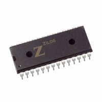
Z8F0213PJ005SC Zilog, Z8F0213PJ005SC Datasheet - Page 130

Z8F0213PJ005SC
Manufacturer Part Number
Z8F0213PJ005SC
Description
IC ENCORE MCU FLASH 2K 28DIP
Manufacturer
Zilog
Series
Encore!® XP®r
Datasheet
1.Z8F0223SB005SG.pdf
(247 pages)
Specifications of Z8F0213PJ005SC
Core Processor
Z8
Core Size
8-Bit
Speed
5MHz
Connectivity
IrDA, UART/USART
Peripherals
Brown-out Detect/Reset, LED, POR, PWM, WDT
Number Of I /o
24
Program Memory Size
2KB (2K x 8)
Program Memory Type
FLASH
Ram Size
512 x 8
Voltage - Supply (vcc/vdd)
2.7 V ~ 3.6 V
Oscillator Type
Internal
Operating Temperature
0°C ~ 70°C
Package / Case
28-DIP (0.600", 15.24mm)
Lead Free Status / RoHS Status
Contains lead / RoHS non-compliant
Eeprom Size
-
Data Converters
-
Other names
269-3461
- Current page: 130 of 247
- Download datasheet (4Mb)
PS024314-0308
Caution:
Continuous Conversion
5. When the conversion is complete, the ADC control logic performs the following
6. If the ADC remains idle for 160 consecutive system clock cycles, it is automatically
When configured for continuous conversion, the ADC continuously performs an analog-
to-digital conversion on the selected analog input. Each new data value over-writes the
previous value stored in the ADC Data registers. An interrupt is generated after each con-
version.
Follow the steps below for setting up the ADC and initiating continuous conversion:
1. Enable the acceptable analog input by configuring the general-purpose I/O pins for
2. Write the
3. Write to the
In CONTINUOUS mode, ADC updates are limited by the input signal bandwidth of the
ADC and the latency of the ADC and its digital filter. Step changes at the input are not
detected at the next output from the ADC. The response of the ADC (in all modes) is lim-
ited by the input signal bandwidth and the latency.
operations:
–
–
powered-down.
alternate function. This action disables the digital input and output driver.
–
The bit fields in the ADC Control register can be written simultaneously:
–
–
–
–
–
11-bit two’s-complement result written to {ADCD_H[7:0], ADCD_L[7:5]}.
CEN resets to 0 to indicate the conversion is complete.
Write the
voltage reference level or to disable the internal reference. The REFSELH bit is
contained in the
Write to the ANAIN[3:0] field to select from the available analog input sources
(different input pins available depending on the device).
Set CONT to 1 to select continuous conversion.
If the internal VREF must be output to a pin, set the REFEXT bit to 1. The
internal voltage reference must be enabled in this case.
Write the REFSELL bit of the pair {REFSELH, REFSELL} to select the internal
voltage reference level or to disable the internal reference. The REFSELL bit is
contained in
Set CEN to 1 to start the conversions.
ADC Control/Status Register 1
ADC Control Register 0
REFSELH
ADC Control Register
ADC Control/Status Register
bit of the pair {
to configure the ADC for continuous conversion.
REFSELH
0.
to configure the ADC:
,
REFSELL
1.
Z8 Encore! XP
} to select the internal
Product Specification
Analog-to-Digital Converter
®
F0823 Series
120
Related parts for Z8F0213PJ005SC
Image
Part Number
Description
Manufacturer
Datasheet
Request
R

Part Number:
Description:
Communication Controllers, ZILOG INTELLIGENT PERIPHERAL CONTROLLER (ZIP)
Manufacturer:
Zilog, Inc.
Datasheet:

Part Number:
Description:
KIT DEV FOR Z8 ENCORE 16K TO 64K
Manufacturer:
Zilog
Datasheet:

Part Number:
Description:
KIT DEV Z8 ENCORE XP 28-PIN
Manufacturer:
Zilog
Datasheet:

Part Number:
Description:
DEV KIT FOR Z8 ENCORE 8K/4K
Manufacturer:
Zilog
Datasheet:

Part Number:
Description:
KIT DEV Z8 ENCORE XP 28-PIN
Manufacturer:
Zilog
Datasheet:

Part Number:
Description:
DEV KIT FOR Z8 ENCORE 4K TO 8K
Manufacturer:
Zilog
Datasheet:

Part Number:
Description:
CMOS Z8 microcontroller. ROM 16 Kbytes, RAM 256 bytes, speed 16 MHz, 32 lines I/O, 3.0V to 5.5V
Manufacturer:
Zilog, Inc.
Datasheet:

Part Number:
Description:
Low-cost microcontroller. 512 bytes ROM, 61 bytes RAM, 8 MHz
Manufacturer:
Zilog, Inc.
Datasheet:

Part Number:
Description:
Z8 4K OTP Microcontroller
Manufacturer:
Zilog, Inc.
Datasheet:

Part Number:
Description:
CMOS SUPER8 ROMLESS MCU
Manufacturer:
Zilog, Inc.
Datasheet:

Part Number:
Description:
SL1866 CMOSZ8 OTP Microcontroller
Manufacturer:
Zilog, Inc.
Datasheet:

Part Number:
Description:
SL1866 CMOSZ8 OTP Microcontroller
Manufacturer:
Zilog, Inc.
Datasheet:

Part Number:
Description:
OTP (KB) = 1, RAM = 125, Speed = 12, I/O = 14, 8-bit Timers = 2, Comm Interfaces Other Features = Por, LV Protect, Voltage = 4.5-5.5V
Manufacturer:
Zilog, Inc.
Datasheet:

Part Number:
Description:
Manufacturer:
Zilog, Inc.
Datasheet:


