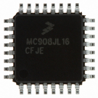
MC908JL16CFJE Freescale Semiconductor, MC908JL16CFJE Datasheet - Page 34

MC908JL16CFJE
Manufacturer Part Number
MC908JL16CFJE
Description
IC MCU 16K FLASH 8MHZ 32-LQFP
Manufacturer
Freescale Semiconductor
Series
HC08r
Datasheet
1.MC908JL16CFJER.pdf
(230 pages)
Specifications of MC908JL16CFJE
Core Processor
HC08
Core Size
8-Bit
Speed
8MHz
Connectivity
I²C, SCI
Peripherals
LED, LVD, POR, PWM
Number Of I /o
26
Program Memory Size
16KB (16K x 8)
Program Memory Type
FLASH
Ram Size
512 x 8
Voltage - Supply (vcc/vdd)
2.7 V ~ 5.5 V
Data Converters
A/D 13x10b
Oscillator Type
Internal
Operating Temperature
-40°C ~ 85°C
Package / Case
32-LQFP
Processor Series
HC08JL
Core
HC08
Data Bus Width
8 bit
Data Ram Size
512 B
Interface Type
SCI
Maximum Clock Frequency
8 MHz
Number Of Programmable I/os
26
Number Of Timers
4
Operating Supply Voltage
2.7 V to 5.5 V
Maximum Operating Temperature
+ 85 C
Mounting Style
SMD/SMT
Development Tools By Supplier
FSICEBASE, DEMO908JL16E, M68CBL05CE
Minimum Operating Temperature
- 40 C
On-chip Adc
13-ch x 10-bit
Controller Family/series
HC08
No. Of I/o's
26
Ram Memory Size
512Byte
Cpu Speed
8MHz
No. Of Timers
2
Embedded Interface Type
I2C, SCI, SPI
Rohs Compliant
Yes
For Use With
DEMO908JL16E - BOARD DEMO FOR MC908JL16
Lead Free Status / RoHS Status
Lead free / RoHS Compliant
Eeprom Size
-
Lead Free Status / Rohs Status
Lead free / RoHS Compliant
Available stocks
Company
Part Number
Manufacturer
Quantity
Price
Company:
Part Number:
MC908JL16CFJE
Manufacturer:
Freescale Semiconductor
Quantity:
1 806
Company:
Part Number:
MC908JL16CFJE
Manufacturer:
Freescale Semiconductor
Quantity:
10 000
Part Number:
MC908JL16CFJE
Manufacturer:
FREESCALE
Quantity:
20 000
Company:
Part Number:
MC908JL16CFJER
Manufacturer:
Freescale Semiconductor
Quantity:
29 890
Company:
Part Number:
MC908JL16CFJER
Manufacturer:
Freescale
Quantity:
198
Company:
Part Number:
MC908JL16CFJER
Manufacturer:
Freescale Semiconductor
Quantity:
10 000
Memory
2.5.2 FLASH Control Register
The FLASH control register (FCLR) controls FLASH program and erase operations.
HVEN — High Voltage Enable Bit
MASS — Mass Erase Control Bit
ERASE — Erase Control Bit
PGM — Program Control Bit
34
This read/write bit enables the charge pump to drive high voltages for program and erase operations
in the array. HVEN can only be set if either PGM = 1 or ERASE = 1 and the proper sequence for
program or erase is followed.
This read/write bit configures the memory for mass erase operation or page erase operation when the
ERASE bit is set.
This read/write bit configures the memory for erase operation. ERASE is interlocked with the PGM bit
such that both bits cannot be equal to 1 or set to 1 at the same time.
This read/write bit configures the memory for program operation. PGM is interlocked with the ERASE
bit such that both bits cannot be equal to 1 or set to 1 at the same time.
1 = High voltage enabled to array and charge pump on
0 = High voltage disabled to array and charge pump off
1 = Mass erase operation selected
0 = Page erase operation selected
1 = Erase operation selected
0 = Erase operation not selected
1 = Program operation selected
0 = Program operation not selected
Address: $FE08
Reset:
Read:
Write:
Bit 7
0
0
Figure 2-3. FLASH Control Register (FLCR)
= Unimplemented
6
0
0
MC68HC908JL16 Data Sheet, Rev. 1.1
5
0
0
4
0
0
HVEN
3
0
MASS
2
0
ERASE
1
0
Freescale Semiconductor
PGM
Bit 0
0


