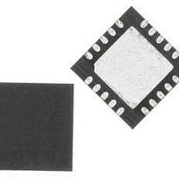
C8051F818-GM Silicon Laboratories Inc, C8051F818-GM Datasheet - Page 125

C8051F818-GM
Manufacturer Part Number
C8051F818-GM
Description
IC MCU 8BIT 8KB FLASH 20QFN
Manufacturer
Silicon Laboratories Inc
Series
C8051F81xr
Datasheet
1.C8051F800DK.pdf
(250 pages)
Specifications of C8051F818-GM
Core Processor
8051
Core Size
8-Bit
Speed
25MHz
Connectivity
SMBus (2-Wire/I²C), SPI, UART/USART
Peripherals
Cap Sense, POR, PWM, WDT
Number Of I /o
17
Program Memory Size
8KB (8K x 8)
Program Memory Type
FLASH
Ram Size
512 x 8
Voltage - Supply (vcc/vdd)
1.8 V ~ 3.6 V
Oscillator Type
Internal
Operating Temperature
-40°C ~ 85°C
Package / Case
20-QFN
Processor Series
C8051F8x
Core
8051
Data Bus Width
16 bit
Data Ram Size
512 B
Interface Type
I2C, SPI, UART
Maximum Clock Frequency
25 MHz
Number Of Programmable I/os
17
Number Of Timers
3
Operating Supply Voltage
1.8 V to 3.6 V
Maximum Operating Temperature
+ 125 C
Mounting Style
SMD/SMT
3rd Party Development Tools
PK51, CA51, A51, ULINK2
Development Tools By Supplier
C8051F800DK
Minimum Operating Temperature
- 55 C
Lead Free Status / RoHS Status
Lead free / RoHS Compliant
Eeprom Size
-
Data Converters
-
Lead Free Status / Rohs Status
Details
Other names
336-1798-5
- Current page: 125 of 250
- Download datasheet (2Mb)
21.2. Power-Fail Reset / V
When a power-down transition or power irregularity causes V
monitor will drive the RST pin low and hold the CIP-51 in a reset state (see Figure 21.2). When V
to a level above V
contents are not altered by the power-fail reset, it is impossible to determine if V
required for data retention. If the PORSF flag reads 1, the data may no longer be valid. The V
enabled and selected as a reset source after power-on resets. Its defined state (enabled/disabled) is not
altered by any other reset source. For example, if the V
is performed, the V
Important Note: If the V
is selected as a reset source. Selecting the V
lized may cause a system reset. In some applications, this reset may be undesirable. If this is not desirable
in the application, a delay should be introduced between enabling the monitor and selecting it as a reset
source. The procedure for enabling the V
state is shown below:
1. Enable the V
2. If necessary, wait for the V
3. Select the V
See Figure 21.2 for V
monitor reset. See Section “7. Electrical Characteristics” on page 39 for complete electrical characteristics
of the V
DD
monitor.
DD
DD
RST
monitor as a reset source (PORSF bit in RSTSRC = 1).
DD
monitor (VDMEN bit in VDM0CN = 1).
, the CIP-51 will be released from the reset state. Even though internal data memory
monitor will still be disabled after the reset.
DD
DD
monitor timing; note that the power-on-reset delay is not incurred after a V
monitor is being turned on from a disabled state, it should be enabled before it
DD
monitor to stabilize.
DD
Monitor
DD
monitor and configuring it as a reset source from a disabled
DD
Rev. 1.0
monitor as a reset source before it is enabled and stabi-
DD
monitor is disabled by code and a software reset
DD
to drop below V
C8051F80x-83x
DD
dropped below the level
RST
, the power supply
DD
DD
monitor is
returns
125
DD
Related parts for C8051F818-GM
Image
Part Number
Description
Manufacturer
Datasheet
Request
R
Part Number:
Description:
SMD/C°/SINGLE-ENDED OUTPUT SILICON OSCILLATOR
Manufacturer:
Silicon Laboratories Inc
Part Number:
Description:
Manufacturer:
Silicon Laboratories Inc
Datasheet:
Part Number:
Description:
N/A N/A/SI4010 AES KEYFOB DEMO WITH LCD RX
Manufacturer:
Silicon Laboratories Inc
Datasheet:
Part Number:
Description:
N/A N/A/SI4010 SIMPLIFIED KEY FOB DEMO WITH LED RX
Manufacturer:
Silicon Laboratories Inc
Datasheet:
Part Number:
Description:
N/A/-40 TO 85 OC/EZLINK MODULE; F930/4432 HIGH BAND (REV E/B1)
Manufacturer:
Silicon Laboratories Inc
Part Number:
Description:
EZLink Module; F930/4432 Low Band (rev e/B1)
Manufacturer:
Silicon Laboratories Inc
Part Number:
Description:
I°/4460 10 DBM RADIO TEST CARD 434 MHZ
Manufacturer:
Silicon Laboratories Inc
Part Number:
Description:
I°/4461 14 DBM RADIO TEST CARD 868 MHZ
Manufacturer:
Silicon Laboratories Inc
Part Number:
Description:
I°/4463 20 DBM RFSWITCH RADIO TEST CARD 460 MHZ
Manufacturer:
Silicon Laboratories Inc
Part Number:
Description:
I°/4463 20 DBM RADIO TEST CARD 868 MHZ
Manufacturer:
Silicon Laboratories Inc
Part Number:
Description:
I°/4463 27 DBM RADIO TEST CARD 868 MHZ
Manufacturer:
Silicon Laboratories Inc
Part Number:
Description:
I°/4463 SKYWORKS 30 DBM RADIO TEST CARD 915 MHZ
Manufacturer:
Silicon Laboratories Inc
Part Number:
Description:
N/A N/A/-40 TO 85 OC/4463 RFMD 30 DBM RADIO TEST CARD 915 MHZ
Manufacturer:
Silicon Laboratories Inc
Part Number:
Description:
I°/4463 20 DBM RADIO TEST CARD 169 MHZ
Manufacturer:
Silicon Laboratories Inc


