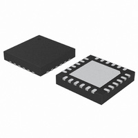
C8051F317-GM Silicon Laboratories Inc, C8051F317-GM Datasheet - Page 131

C8051F317-GM
Manufacturer Part Number
C8051F317-GM
Description
IC 8051 MCU FLASH 16KB 24QFN
Manufacturer
Silicon Laboratories Inc
Series
C8051F31xr
Specifications of C8051F317-GM
Program Memory Type
FLASH
Program Memory Size
16KB (16K x 8)
Package / Case
24-QFN
Core Processor
8051
Core Size
8-Bit
Speed
25MHz
Connectivity
SMBus (2-Wire/I²C), SPI, UART/USART
Peripherals
POR, PWM, WDT
Number Of I /o
21
Ram Size
1.25K x 8
Voltage - Supply (vcc/vdd)
2.7 V ~ 3.6 V
Oscillator Type
Internal
Operating Temperature
-40°C ~ 85°C
Processor Series
C8051F3x
Core
8051
Data Bus Width
8 bit
Data Ram Size
1.25 KB
Interface Type
I2C, SMBus, SPI, UART
Maximum Clock Frequency
25 MHz
Number Of Programmable I/os
21
Number Of Timers
5
Operating Supply Voltage
2.7 V to 3.6 V
Maximum Operating Temperature
+ 85 C
Mounting Style
SMD/SMT
3rd Party Development Tools
PK51, CA51, A51, ULINK2
Development Tools By Supplier
C8051F310DK
Minimum Operating Temperature
- 40 C
On-chip Adc
10 bit
Lead Free Status / RoHS Status
Lead free / RoHS Compliant
For Use With
770-1006 - ISP 4PORT FOR SILABS C8051F MCU
Eeprom Size
-
Data Converters
-
Lead Free Status / Rohs Status
Lead free / RoHS Compliant
Other names
336-1282-5
Available stocks
Company
Part Number
Manufacturer
Quantity
Price
Part Number:
C8051F317-GMR
Manufacturer:
SILICON LABS/芯科
Quantity:
20 000
13.1. Priority Crossbar Decoder
The Priority Crossbar Decoder (Figure 13.3) assigns a priority to each I/O function, starting at the top with
UART0. When a digital resource is selected, the least-significant unassigned Port pin is assigned to that
resource (excluding UART0, which is always at pins 4 and 5). If a Port pin is assigned, the Crossbar skips
that pin when assigning the next selected resource. Additionally, the Crossbar will skip Port pins whose
associated bits in the PnSKIP registers are set. The PnSKIP registers allow software to skip Port pins that
are to be used for analog input, dedicated functions, or GPIO.
Important Note on Crossbar Configuration: If a Port pin is claimed by a peripheral without use of the
Crossbar, its corresponding PnSKIP bit should be set. This applies to P0.0 if VREF is used, P0.3 and/or
P0.2 if the external oscillator circuit is enabled, P0.6 if the ADC is configured to use the external conversion
start signal (CNVSTR), and any selected ADC or Comparator inputs. The Crossbar skips selected pins as
if they were already assigned, and moves to the next unassigned pin. Figure 13.3 shows the Crossbar
Decoder priority with no Port pins skipped (P0SKIP, P1SKIP, P2SKIP = 0x00); Figure 13.4 shows the
Crossbar Decoder priority with the XTAL1 (P0.2) and XTAL2 (P0.3) pins skipped (P0SKIP = 0x0C to skip
P0.2 and P0.3 for XTAL use).
SF Signals
PIN I/O
TX0
RX0
SCK
MISO
MOSI
NSS*
SDA
SCL
CP0
CP0A
CP1
CP1A
SYSCLK
CEX0
CEX1
CEX2
CEX3
CEX4
ECI
T0
T1
SF Signals
*Note: NSS is only pinned out in 4-wire SPI mode.
Note: P1.6,P1.7,P2.6,P2.7 only available on the C8051F310/1/2/3/4/5; P1SKIP[7:6] should always be
set to 11b for the C8051F316/7 devices.
Port pin potentially available to peripheral
Special Function Signals are not assigned by the Crossbar. When these signals are enabled, the Crossbar must
be manually configured to skip their corresponding port pins.
Figure 13.3. Crossbar Priority Decoder with No Pins Skipped
0
0
1
0
2
0
P0SKIP[0:7]
3
0
P0
4
0
5
0
6
0
7
0
0
0
1
0
Rev. 1.7
2
0
P1SKIP[0:7]
3
0
P1
C8051F310/1/2/3/4/5/6/7
4
0
5
0
6
0
7
0
0
0
P2SKIP[0:3]
1
0
2
0
3
0
P2
4
5
6
7
131


