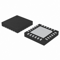
C8051F317-GM Silicon Laboratories Inc, C8051F317-GM Datasheet - Page 142

C8051F317-GM
Manufacturer Part Number
C8051F317-GM
Description
IC 8051 MCU FLASH 16KB 24QFN
Manufacturer
Silicon Laboratories Inc
Series
C8051F31xr
Specifications of C8051F317-GM
Program Memory Type
FLASH
Program Memory Size
16KB (16K x 8)
Package / Case
24-QFN
Core Processor
8051
Core Size
8-Bit
Speed
25MHz
Connectivity
SMBus (2-Wire/I²C), SPI, UART/USART
Peripherals
POR, PWM, WDT
Number Of I /o
21
Ram Size
1.25K x 8
Voltage - Supply (vcc/vdd)
2.7 V ~ 3.6 V
Oscillator Type
Internal
Operating Temperature
-40°C ~ 85°C
Processor Series
C8051F3x
Core
8051
Data Bus Width
8 bit
Data Ram Size
1.25 KB
Interface Type
I2C, SMBus, SPI, UART
Maximum Clock Frequency
25 MHz
Number Of Programmable I/os
21
Number Of Timers
5
Operating Supply Voltage
2.7 V to 3.6 V
Maximum Operating Temperature
+ 85 C
Mounting Style
SMD/SMT
3rd Party Development Tools
PK51, CA51, A51, ULINK2
Development Tools By Supplier
C8051F310DK
Minimum Operating Temperature
- 40 C
On-chip Adc
10 bit
Lead Free Status / RoHS Status
Lead free / RoHS Compliant
For Use With
770-1006 - ISP 4PORT FOR SILABS C8051F MCU
Eeprom Size
-
Data Converters
-
Lead Free Status / Rohs Status
Lead free / RoHS Compliant
Other names
336-1282-5
Available stocks
Company
Part Number
Manufacturer
Quantity
Price
Part Number:
C8051F317-GMR
Manufacturer:
SILICON LABS/芯科
Quantity:
20 000
C8051F310/1/2/3/4/5/6/7
142
Note:
Note:
Bits7–0: P3.[7:0]
Bits7–5: UNUSED. Read = 000b; Write = don’t care.
Bits4–0: Input Configuration Bits for P3.4–P3.0 (respectively).
P3.7
R/W
R/W
Bit7
Bit7
-
Write - Output appears on I/O pins.
0: Logic Low Output.
1: Logic High Output (high impedance if corresponding P3MDOUT.n bit = 0).
Read - Always reads ‘1’ if selected as analog input in register P3MDIN. Directly reads Port
pin when configured as digital input.
0: P3.n pin is logic low.
1: P3.n pin is logic high.
Only P3.0–P3.4 are associated with Port pins on C8051F310/2/4 devices; Only P3.0 is associated with a
Port pin on C8051F311/3/5/6/7 devices.
Port pins configured as analog inputs have their weak pullup, digital driver, and digital
receiver disabled.
0: Corresponding P3.n pin is configured as an analog input.
1: Corresponding P3.n pin is not configured as an analog input.
Only P3.0–P3.4 are associated with Port pins on C8051F310/2/4 devices; Only P3.0 is associated with a
Port pin on C8051F311/3/5/6/7 devices.
P3.6
R/W
R/W
Bit6
Bit6
-
SFR Definition 13.16. P3MDIN: Port3 Input Mode
P3.5
R/W
R/W
Bit5
Bit5
-
SFR Definition 13.15. P3: Port3
P3.4
R/W
R/W
Bit4
Bit4
Rev. 1.7
P3.3
R/W
R/W
Bit3
Bit3
P3.2
R/W
R/W
Bit2
Bit2
P3.1
R/W
R/W
Bit1
Bit1
(bit addressable)
P3.0
R/W
R/W
Bit0
Bit0
SFR Address:
SFR Address:
Reset Value
Reset Value
11111111
11111111
0xB0
0xF4


