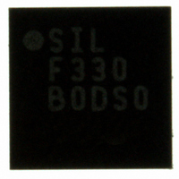
C8051F330-GM Silicon Laboratories Inc, C8051F330-GM Datasheet - Page 63

C8051F330-GM
Manufacturer Part Number
C8051F330-GM
Description
IC 8051 MCU 8K FLASH 20MLP
Manufacturer
Silicon Laboratories Inc
Series
C8051F33xr
Specifications of C8051F330-GM
Program Memory Type
FLASH
Program Memory Size
8KB (8K x 8)
Package / Case
20-QFN
Core Processor
8051
Core Size
8-Bit
Speed
25MHz
Connectivity
SMBus (2-Wire/I²C), SPI, UART/USART
Peripherals
POR, PWM, Temp Sensor, WDT
Number Of I /o
17
Ram Size
768 x 8
Voltage - Supply (vcc/vdd)
2.7 V ~ 3.6 V
Data Converters
A/D 16x10b; D/A 1x10b
Oscillator Type
Internal
Operating Temperature
-40°C ~ 85°C
Processor Series
C8051F3x
Core
8051
Data Bus Width
8 bit
Data Ram Size
768 B
Interface Type
I2C/SMBus/SPI/UART
Maximum Clock Frequency
25 MHz
Number Of Programmable I/os
17
Number Of Timers
4
Operating Supply Voltage
2.7 V to 3.6 V
Maximum Operating Temperature
+ 85 C
Mounting Style
SMD/SMT
3rd Party Development Tools
KSK-SL-TOOLSTICK, PK51, CA51, A51, ULINK2
Development Tools By Supplier
C8051F330DK
Minimum Operating Temperature
- 40 C
On-chip Adc
16-ch x 10-bit
On-chip Dac
1-ch x 10-bit
No. Of I/o's
17
Ram Memory Size
768Byte
Cpu Speed
25MHz
No. Of Timers
4
Rohs Compliant
Yes
Lead Free Status / RoHS Status
Lead free / RoHS Compliant
For Use With
336-1541 - KIT TOOL EVAL SYS IN A USB STICK770-1006 - ISP 4PORT FOR SILABS C8051F MCU336-1451 - ADAPTER PROGRAM TOOLSTICK F330336-1346 - DAUGHTER CARD TOOLSTICK F330336-1264 - DEV KIT FOR C8051F330/F331
Eeprom Size
-
Lead Free Status / Rohs Status
Lead free / RoHS Compliant
Other names
336-1262
Available stocks
Company
Part Number
Manufacturer
Quantity
Price
Company:
Part Number:
C8051F330-GM
Manufacturer:
SiliconL
Quantity:
6 420
Company:
Part Number:
C8051F330-GM
Manufacturer:
SILICON
Quantity:
121
Part Number:
C8051F330-GM
Manufacturer:
SILICON LABS/芯科
Quantity:
20 000
Company:
Part Number:
C8051F330-GM-15T
Manufacturer:
SILICON
Quantity:
3 741
Part Number:
C8051F330-GMR
Manufacturer:
SILICON LABS/芯科
Quantity:
20 000
C8051F330/1/2/3/4/5
The Comparator output can be polled in software, used as an interrupt source, and/or routed to a Port pin.
When routed to a Port pin, the Comparator output is available asynchronous or synchronous to the system
clock; the asynchronous output is available even in STOP mode (with no system clock active). When dis-
abled, the Comparator output (if assigned to a Port I/O pin via the Crossbar) defaults to the logic low state,
and its supply current falls to less than 100 nA. See
page 125
externally driven from –0.25 V to (VDD) + 0.25 V without damage or upset. The complete Comparator
electrical specifications are given in Table 8.1.
The Comparator response time may be configured in software via the CPT0MD register (see SFR Defini-
tion 8.3). Selecting a longer response time reduces the Comparator supply current. See Table 8.1 for com-
plete timing and power consumption specifications.
The Comparator hysteresis is software-programmable via its Comparator Control register CPT0CN. The
user can program both the amount of hysteresis voltage (referred to the input voltage) and the positive and
negative-going symmetry of this hysteresis around the threshold voltage.
The Comparator hysteresis is programmed using Bits3–0 in the Comparator Control Register CPT0CN
(shown in SFR Definition 8.1). The amount of negative hysteresis voltage is determined by the settings of
the CP0HYN bits. As shown in Figure 8.2, settings of 20, 10 or 5 mV of negative hysteresis can be pro-
grammed, or negative hysteresis can be disabled. In a similar way, the amount of positive hysteresis is
determined by the setting the CP0HYP bits.
Comparator interrupts can be generated on both rising-edge and falling-edge output transitions. (For Inter-
rupt enable and priority control, see Section “8.3. Interrupt Handler” on page 58). The CP0FIF flag is set to
66
for details on configuring Comparator outputs via the digital Crossbar. Comparator inputs can be
(Programmed with CP0HYP Bits)
Positive Hysteresis Voltage
INPUTS
OUTPUT
VIN+
VIN-
CIRCUIT CONFIGURATION
Positive Hysteresis
CP0-
CP0+
VIN+
VIN-
Disabled
V
OL
Figure 8.2. Comparator Hysteresis Plot
V
OH
+
_
CP0
Positive Hysteresis
Maximum
OUT
Rev. 1.7
Negative Hysteresis
Disabled
Section “14.1. Priority Crossbar Decoder” on
Negative Hysteresis
(Programmed by CP0HYN Bits)
Maximum
Negative Hysteresis Voltage


