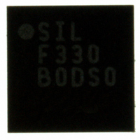
C8051F330-GM Silicon Laboratories Inc, C8051F330-GM Datasheet - Page 84

C8051F330-GM
Manufacturer Part Number
C8051F330-GM
Description
IC 8051 MCU 8K FLASH 20MLP
Manufacturer
Silicon Laboratories Inc
Series
C8051F33xr
Specifications of C8051F330-GM
Program Memory Type
FLASH
Program Memory Size
8KB (8K x 8)
Package / Case
20-QFN
Core Processor
8051
Core Size
8-Bit
Speed
25MHz
Connectivity
SMBus (2-Wire/I²C), SPI, UART/USART
Peripherals
POR, PWM, Temp Sensor, WDT
Number Of I /o
17
Ram Size
768 x 8
Voltage - Supply (vcc/vdd)
2.7 V ~ 3.6 V
Data Converters
A/D 16x10b; D/A 1x10b
Oscillator Type
Internal
Operating Temperature
-40°C ~ 85°C
Processor Series
C8051F3x
Core
8051
Data Bus Width
8 bit
Data Ram Size
768 B
Interface Type
I2C/SMBus/SPI/UART
Maximum Clock Frequency
25 MHz
Number Of Programmable I/os
17
Number Of Timers
4
Operating Supply Voltage
2.7 V to 3.6 V
Maximum Operating Temperature
+ 85 C
Mounting Style
SMD/SMT
3rd Party Development Tools
KSK-SL-TOOLSTICK, PK51, CA51, A51, ULINK2
Development Tools By Supplier
C8051F330DK
Minimum Operating Temperature
- 40 C
On-chip Adc
16-ch x 10-bit
On-chip Dac
1-ch x 10-bit
No. Of I/o's
17
Ram Memory Size
768Byte
Cpu Speed
25MHz
No. Of Timers
4
Rohs Compliant
Yes
Lead Free Status / RoHS Status
Lead free / RoHS Compliant
For Use With
336-1541 - KIT TOOL EVAL SYS IN A USB STICK770-1006 - ISP 4PORT FOR SILABS C8051F MCU336-1451 - ADAPTER PROGRAM TOOLSTICK F330336-1346 - DAUGHTER CARD TOOLSTICK F330336-1264 - DEV KIT FOR C8051F330/F331
Eeprom Size
-
Lead Free Status / Rohs Status
Lead free / RoHS Compliant
Other names
336-1262
Available stocks
Company
Part Number
Manufacturer
Quantity
Price
Company:
Part Number:
C8051F330-GM
Manufacturer:
SiliconL
Quantity:
6 420
Company:
Part Number:
C8051F330-GM
Manufacturer:
SILICON
Quantity:
121
Part Number:
C8051F330-GM
Manufacturer:
SILICON LABS/芯科
Quantity:
20 000
Company:
Part Number:
C8051F330-GM-15T
Manufacturer:
SILICON
Quantity:
3 741
Part Number:
C8051F330-GMR
Manufacturer:
SILICON LABS/芯科
Quantity:
20 000
9.3.2. External Interrupts
The /INT0 and /INT1 external interrupt sources are configurable as active high or low, edge or level sensi-
tive. The IN0PL (/INT0 Polarity) and IN1PL (/INT1 Polarity) bits in the IT01CF register select active high or
active low; the IT0 and IT1 bits in TCON
or edge sensitive. The table below lists the possible configurations.
/INT0 and /INT1 are assigned to Port pins as defined in the IT01CF register (see SFR Definition 9.11).
Note that /INT0 and /INT0 Port pin assignments are independent of any Crossbar assignments. /INT0 and
/INT1 will monitor their assigned Port pins without disturbing the peripheral that was assigned the Port pin
via the Crossbar. To assign a Port pin only to /INT0 and/or /INT1, configure the Crossbar to skip the
selected pin(s). This is accomplished by setting the associated bit in register XBR0 (see
“14.1. Priority Crossbar Decoder” on page 125
IE0 (TCON.1) and IE1 (TCON.3) serve as the interrupt-pending flags for the /INT0 and /INT1 external
interrupts, respectively. If an /INT0 or /INT1 external interrupt is configured as edge-sensitive, the corre-
sponding interrupt-pending flag is automatically cleared by the hardware when the CPU vectors to the ISR.
When configured as level sensitive, the interrupt-pending flag remains logic 1 while the input is active as
defined by the corresponding polarity bit (IN0PL or IN1PL); the flag remains logic 0 while the input is inac-
tive. The external interrupt source must hold the input active until the interrupt request is recognized. It
must then deactivate the interrupt request before execution of the ISR completes or another interrupt
request will be generated.
9.3.3. Interrupt Priorities
Each interrupt source can be individually programmed to one of two priority levels: low or high. A low prior-
ity interrupt service routine can be preempted by a high priority interrupt. A high priority interrupt cannot be
preempted. Each interrupt has an associated interrupt priority bit in an SFR (IP or EIP1) used to configure
its priority level. Low priority is the default. If two interrupts are recognized simultaneously, the interrupt with
the higher priority is serviced first. If both interrupts have the same priority level, a fixed priority order is
used to arbitrate, given in Table 9.4.
9.3.4. Interrupt Latency
Interrupt response time depends on the state of the CPU when the interrupt occurs. Pending interrupts are
sampled and priority decoded each system clock cycle. Therefore, the fastest possible response time is 5
system clock cycles: 1 clock cycle to detect the interrupt and 4 clock cycles to complete the LCALL to the
ISR. If an interrupt is pending when a RETI is executed, a single instruction is executed before an LCALL
is made to service the pending interrupt. Therefore, the maximum response time for an interrupt (when no
other interrupt is currently being serviced or the new interrupt is of greater priority) occurs when the CPU is
performing an RETI instruction followed by a DIV as the next instruction. In this case, the response time is
18 system clock cycles: 1 clock cycle to detect the interrupt, 5 clock cycles to execute the RETI, 8 clock
cycles to complete the DIV instruction and 4 clock cycles to execute the LCALL to the ISR. If the CPU is
executing an ISR for an interrupt with equal or higher priority, the new interrupt will not be serviced until the
current ISR completes, including the RETI and following instruction.
IT0
1
1
0
0
IN0PL
0
1
0
1
Active low, edge sensitive
Active high, edge sensitive
Active low, level sensitive
Active high, level sensitive
/INT0 Interrupt
(Section “18.1. Timer 0 and Timer 1” on page
Rev. 1.7
for complete details on configuring the Crossbar).
IT1
1
1
0
0
C8051F330/1/2/3/4/5
IN1PL
0
1
0
1
Active low, edge sensitive
Active high, edge sensitive
Active low, level sensitive
Active high, level sensitive
/INT1 Interrupt
177) select level
Section
87


