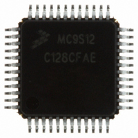
MC9S12C128CFAE Freescale Semiconductor, MC9S12C128CFAE Datasheet - Page 141

MC9S12C128CFAE
Manufacturer Part Number
MC9S12C128CFAE
Description
IC MCU 16BIT 4K FLASH 48-LQFP
Manufacturer
Freescale Semiconductor
Series
HCS12r
Specifications of MC9S12C128CFAE
Core Processor
HCS12
Core Size
16-Bit
Speed
25MHz
Connectivity
CAN, EBI/EMI, SCI, SPI
Peripherals
POR, PWM, WDT
Number Of I /o
31
Program Memory Size
128KB (128K x 8)
Program Memory Type
FLASH
Ram Size
4K x 8
Voltage - Supply (vcc/vdd)
2.35 V ~ 5.5 V
Data Converters
A/D 8x10b
Oscillator Type
Internal
Operating Temperature
-40°C ~ 85°C
Package / Case
48-LQFP
Processor Series
S12C
Core
HCS12
Data Bus Width
16 bit
Data Ram Size
4 KB
Interface Type
CAN/SCI/SPI
Maximum Clock Frequency
25 MHz
Number Of Programmable I/os
31
Number Of Timers
8
Maximum Operating Temperature
+ 85 C
Mounting Style
SMD/SMT
3rd Party Development Tools
EWHCS12
Development Tools By Supplier
M68EVB912C32EE
Minimum Operating Temperature
- 40 C
On-chip Adc
8-ch x 10-bit
Lead Free Status / RoHS Status
Lead free / RoHS Compliant
Eeprom Size
-
Lead Free Status / Rohs Status
Lead free / RoHS Compliant
Available stocks
Company
Part Number
Manufacturer
Quantity
Price
Company:
Part Number:
MC9S12C128CFAE
Manufacturer:
Freescale Semiconductor
Quantity:
10 000
- Current page: 141 of 690
- Download datasheet (4Mb)
4.3.2.8
Read: Anytime (provided this register is in the map).
Write: Each bit has specific write conditions. Please refer to the descriptions of each bit on the following
pages.
Port E serves as general-purpose I/O or as system and bus control signals. The PEAR register is used to
choose between the general-purpose I/O function and the alternate control functions. When an alternate
control function is selected, the associated DDRE bits are overridden.
The reset condition of this register depends on the mode of operation because bus control signals are
needed immediately after reset in some modes. In normal single-chip mode, no external bus control signals
are needed so all of port E is configured for general-purpose I/O. In normal expanded modes, only the E
clock is configured for its alternate bus control function and the other bits of port E are configured for
general-purpose I/O. As the reset vector is located in external memory, the E clock is required for this
access. R/W is only needed by the system when there are external writable resources. If the normal
expanded system needs any other bus control signals, PEAR would need to be written before any access
that needed the additional signals. In special test and emulation modes, IPIPE1, IPIPE0, E, LSTRB, and
R/W are configured out of reset as bus control signals.
This register is not in the on-chip memory map in expanded and special peripheral modes. Therefore, these
accesses will be echoed externally.
Freescale Semiconductor
Module Base + 0x000A
Starting address location affected by INITRG register setting.
Normal Expanded Wide
Emulation Expanded
Emulation Expanded
Special Single Chip
Normal Single Chip
Normal Expanded
Special Test
Peripheral
Port E Assignment Register (PEAR)
Narrow
Narrow
Reset
Wide
W
R
NOACCE
0
0
0
1
1
0
0
0
7
Figure 4-12. Port E Assignment Register (PEAR)
= Unimplemented or Reserved
MC9S12C-Family / MC9S12GC-Family
0
0
0
0
0
0
0
0
0
6
PIPOE
0
1
0
1
1
0
0
0
5
Rev 01.24
NECLK
4
0
0
0
0
0
1
0
0
Chapter 4 Multiplexed External Bus Interface (MEBIV3)
LSTRE
0
1
0
1
1
0
0
0
3
RDWE
0
1
0
1
1
0
0
0
2
0
0
0
0
0
0
0
0
0
1
0
0
0
0
0
0
0
0
0
0
141
Related parts for MC9S12C128CFAE
Image
Part Number
Description
Manufacturer
Datasheet
Request
R
Part Number:
Description:
Manufacturer:
Freescale Semiconductor, Inc
Datasheet:
Part Number:
Description:
Manufacturer:
Freescale Semiconductor, Inc
Datasheet:
Part Number:
Description:
Manufacturer:
Freescale Semiconductor, Inc
Datasheet:
Part Number:
Description:
Manufacturer:
Freescale Semiconductor, Inc
Datasheet:
Part Number:
Description:
Manufacturer:
Freescale Semiconductor, Inc
Datasheet:
Part Number:
Description:
Manufacturer:
Freescale Semiconductor, Inc
Datasheet:
Part Number:
Description:
Manufacturer:
Freescale Semiconductor, Inc
Datasheet:
Part Number:
Description:
Manufacturer:
Freescale Semiconductor, Inc
Datasheet:
Part Number:
Description:
Manufacturer:
Freescale Semiconductor, Inc
Datasheet:
Part Number:
Description:
Manufacturer:
Freescale Semiconductor, Inc
Datasheet:
Part Number:
Description:
Manufacturer:
Freescale Semiconductor, Inc
Datasheet:
Part Number:
Description:
Manufacturer:
Freescale Semiconductor, Inc
Datasheet:
Part Number:
Description:
Manufacturer:
Freescale Semiconductor, Inc
Datasheet:
Part Number:
Description:
Manufacturer:
Freescale Semiconductor, Inc
Datasheet:
Part Number:
Description:
Manufacturer:
Freescale Semiconductor, Inc
Datasheet:


