MC9S12C128CFAE Freescale Semiconductor, MC9S12C128CFAE Datasheet - Page 461
MC9S12C128CFAE
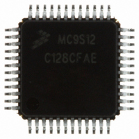
Manufacturer Part Number
MC9S12C128CFAE
Description
IC MCU 16BIT 4K FLASH 48-LQFP
Manufacturer
Freescale Semiconductor
Series
HCS12r
Specifications of MC9S12C128CFAE
Core Processor
HCS12
Core Size
16-Bit
Speed
25MHz
Connectivity
CAN, EBI/EMI, SCI, SPI
Peripherals
POR, PWM, WDT
Number Of I /o
31
Program Memory Size
128KB (128K x 8)
Program Memory Type
FLASH
Ram Size
4K x 8
Voltage - Supply (vcc/vdd)
2.35 V ~ 5.5 V
Data Converters
A/D 8x10b
Oscillator Type
Internal
Operating Temperature
-40°C ~ 85°C
Package / Case
48-LQFP
Processor Series
S12C
Core
HCS12
Data Bus Width
16 bit
Data Ram Size
4 KB
Interface Type
CAN/SCI/SPI
Maximum Clock Frequency
25 MHz
Number Of Programmable I/os
31
Number Of Timers
8
Maximum Operating Temperature
+ 85 C
Mounting Style
SMD/SMT
3rd Party Development Tools
EWHCS12
Development Tools By Supplier
M68EVB912C32EE
Minimum Operating Temperature
- 40 C
On-chip Adc
8-ch x 10-bit
Lead Free Status / RoHS Status
Lead free / RoHS Compliant
Eeprom Size
-
Lead Free Status / Rohs Status
Lead free / RoHS Compliant
Available stocks
Company
Part Number
Manufacturer
Quantity
Price

Company:
Part Number:
MC9S12C128CFAE
Manufacturer:
Freescale Semiconductor
Quantity:
10 000


15.4.6
Setting the PAMOD bit configures the pulse accumulator for gated time accumulation operation. An active
level on the PACNT input pin enables a divided-by-64 clock to drive the pulse accumulator. The PEDGE
bit selects low levels or high levels to enable the divided-by-64 clock.
The trailing edge of the active level at the IOC7 pin sets the PAIF. The PAI bit enables the PAIF flag to
generate interrupt requests.
The pulse accumulator counter register reflect the number of pulses from the divided-by-64 clock since the
last reset.
15.5
The reset state of each individual bit is listed within
which details the registers and their bit fields.
15.6
This section describes interrupts originated by the TIM16B8CV1 block.
generated by the TIM16B8CV1 to communicate with the MCU.
The TIM16B8CV1 uses a total of 11 interrupt vectors. The interrupt vector offsets and interrupt numbers
are chip dependent.
15.6.1
This active high outputs will be asserted by the module to request a timer channel 7 – 0 interrupt to be
serviced by the system controller.
Freescale Semiconductor
1. Chip Dependent.
Interrupt
C[7:0]F
PAOVF
PAOVI
TOF
Resets
Interrupts
Gated Time Accumulation Mode
Channel [7:0] Interrupt (C[7:0]F)
The timer prescaler generates the divided-by-64 clock. If the timer is not
active, there is no divided-by-64 clock.
Offset
(1)
—
—
—
—
Vector
—
—
—
—
1
Table 15-23. TIM16B8CV1 Interrupts
Priority
MC9S12C-Family / MC9S12GC-Family
—
—
—
—
1
Timer Channel 7–0
Pulse Accumulator
Pulse Accumulator
Timer Overflow
Rev 01.24
NOTE
Section 15.3, “Memory Map and Register Definition”
Overflow
Source
Input
Chapter 15 Timer Module (TIM16B8CV1) Block Description
Active high pulse accumulator input interrupt
Active high timer channel interrupts 7–0
Pulse accumulator overflow interrupt
Table 15-23
Timer Overflow interrupt
Description
lists the interrupts
461
Related parts for MC9S12C128CFAE
Image
Part Number
Description
Manufacturer
Datasheet
Request
R

Part Number:
Description:
Manufacturer:
Freescale Semiconductor, Inc
Datasheet:
Part Number:
Description:
Manufacturer:
Freescale Semiconductor, Inc
Datasheet:
Part Number:
Description:
Manufacturer:
Freescale Semiconductor, Inc
Datasheet:
Part Number:
Description:
Manufacturer:
Freescale Semiconductor, Inc
Datasheet:
Part Number:
Description:
Manufacturer:
Freescale Semiconductor, Inc
Datasheet:
Part Number:
Description:
Manufacturer:
Freescale Semiconductor, Inc
Datasheet:
Part Number:
Description:
Manufacturer:
Freescale Semiconductor, Inc
Datasheet:
Part Number:
Description:
Manufacturer:
Freescale Semiconductor, Inc
Datasheet:
Part Number:
Description:
Manufacturer:
Freescale Semiconductor, Inc
Datasheet:
Part Number:
Description:
Manufacturer:
Freescale Semiconductor, Inc
Datasheet:
Part Number:
Description:
Manufacturer:
Freescale Semiconductor, Inc
Datasheet:
Part Number:
Description:
Manufacturer:
Freescale Semiconductor, Inc
Datasheet:
Part Number:
Description:
Manufacturer:
Freescale Semiconductor, Inc
Datasheet:
Part Number:
Description:
Manufacturer:
Freescale Semiconductor, Inc
Datasheet:
Part Number:
Description:
Manufacturer:
Freescale Semiconductor, Inc
Datasheet: