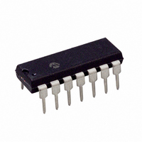
PIC16F526-I/P Microchip Technology, PIC16F526-I/P Datasheet - Page 19

PIC16F526-I/P
Manufacturer Part Number
PIC16F526-I/P
Description
IC PIC MCU FLASH 1KX12 14DIP
Manufacturer
Microchip Technology
Series
PIC® 16Fr
Datasheets
1.PIC16F526-ISL.pdf
(122 pages)
2.PIC16F526-ISL.pdf
(22 pages)
3.PIC16F526-IP.pdf
(104 pages)
Specifications of PIC16F526-I/P
Program Memory Type
FLASH
Program Memory Size
1.5KB (1K x 12)
Package / Case
14-DIP (0.300", 7.62mm)
Core Processor
PIC
Core Size
8-Bit
Speed
20MHz
Peripherals
POR, WDT
Number Of I /o
11
Ram Size
67 x 8
Voltage - Supply (vcc/vdd)
2 V ~ 5.5 V
Data Converters
A/D 3x8b
Oscillator Type
Internal
Operating Temperature
-40°C ~ 85°C
Processor Series
PIC16F
Core
PIC
Data Bus Width
8 bit
Data Ram Size
67 B
Maximum Clock Frequency
20 MHz
Number Of Programmable I/os
12
Number Of Timers
1
Maximum Operating Temperature
+ 85 C
Mounting Style
Through Hole
3rd Party Development Tools
52715-96, 52716-328, 52717-734
Development Tools By Supplier
PG164130, DV164035, DV244005, DV164005, PG164120, ICE2000
Minimum Operating Temperature
- 40 C
On-chip Adc
8 bit, 3 Channel
Lead Free Status / RoHS Status
Lead free / RoHS Compliant
For Use With
AC162096 - HEADER MPLAB ICD2 PIC16F526 8/14
Eeprom Size
-
Connectivity
-
Lead Free Status / Rohs Status
Lead free / RoHS Compliant
6.0
TABLE 6-1:
© 2007 Microchip Technology Inc.
Genera
V
V
T
V
V
V
V
I
I
I
T
T
T
Serial Program/Verify
T
T
T
T
T
T
T
DDPROG
DDERA
PP
SET
ERA
VHHR
PROG
PPDP
HLD
HLD
DLY
DLY
DLY
DIS
IHH
IHL
IH
IL
DDOK
PROG
Sym.
1
1
1
1
2
3
0
1
PROGRAM/VERIFY MODE ELECTRICAL CHARACTERISTICS
l
V
mode entry
Voltage on MCLR to be in Normal mode
MCLR rise time (V
entry
Clock (RB1) and Data (RB0) input high-level
Clock (RB1) and Data (RB0) input low-level
Minimum V
High voltage on MCLR for programming
I
program memory
I
memory
MCLR pin current during Program/Verify mode
Programming time
Hold time after V
ISPCLK, ISPDATA hold time after MCLR↑
(Program/Verify mode selection pattern setup
time)
Data in setup time before clock↓
Data in hold time after clock↓
Data input not driven to next clock input (delay
required between command/data or
command/command)
Delay between clock↓ to clock↑ of next
command or data
Clock↑ to data out valid (during Read Data)
Bulk Erase Time
High Voltage Discharge Time
DD
DD
PP
level for programming operations,
level for Bulk Erase operations, program
High voltage on MCLR for Program/Verify
AC/DC TIMING REQUIREMENTS
DD
Characteristics
to perform Bulk Erase
PP
SS
↑
to V
HH
) for Test mode
AC TARGETS
0.85*V
Min.
1000
12.5
12.5
V
100
100
100
4.5
1.0
1.0
—
—
—
—
—
80
5
5
4
SS
DD
Typ.
13.0
4.0
—
—
—
—
—
—
—
—
—
—
—
—
—
—
—
—
—
—
V
0.15*V
DD
Max.
2000
13.5
13.5
1.0
5.5
1.8
1.8
0.4
10
—
—
—
—
—
—
—
—
—
+ 1.0
DD
PIC16F526
Units
mA
mA
mA
ms
μs
μs
μs
μs
ns
ns
μs
μs
ns
μs
V
V
V
V
V
V
Total time to per-
form both stages
of Bulk Erase and
accept the next
command.
Time to dis-
charge high
voltage.
DS41317B-page 19
Conditions


