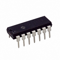
PIC16F526-I/P Microchip Technology, PIC16F526-I/P Datasheet - Page 2

PIC16F526-I/P
Manufacturer Part Number
PIC16F526-I/P
Description
IC PIC MCU FLASH 1KX12 14DIP
Manufacturer
Microchip Technology
Series
PIC® 16Fr
Datasheets
1.PIC16F526-ISL.pdf
(122 pages)
2.PIC16F526-ISL.pdf
(22 pages)
3.PIC16F526-IP.pdf
(104 pages)
Specifications of PIC16F526-I/P
Program Memory Type
FLASH
Program Memory Size
1.5KB (1K x 12)
Package / Case
14-DIP (0.300", 7.62mm)
Core Processor
PIC
Core Size
8-Bit
Speed
20MHz
Peripherals
POR, WDT
Number Of I /o
11
Ram Size
67 x 8
Voltage - Supply (vcc/vdd)
2 V ~ 5.5 V
Data Converters
A/D 3x8b
Oscillator Type
Internal
Operating Temperature
-40°C ~ 85°C
Processor Series
PIC16F
Core
PIC
Data Bus Width
8 bit
Data Ram Size
67 B
Maximum Clock Frequency
20 MHz
Number Of Programmable I/os
12
Number Of Timers
1
Maximum Operating Temperature
+ 85 C
Mounting Style
Through Hole
3rd Party Development Tools
52715-96, 52716-328, 52717-734
Development Tools By Supplier
PG164130, DV164035, DV244005, DV164005, PG164120, ICE2000
Minimum Operating Temperature
- 40 C
On-chip Adc
8 bit, 3 Channel
Lead Free Status / RoHS Status
Lead free / RoHS Compliant
For Use With
AC162096 - HEADER MPLAB ICD2 PIC16F526 8/14
Eeprom Size
-
Connectivity
-
Lead Free Status / Rohs Status
Lead free / RoHS Compliant
PIC16F526
2.0
The Program Memory map of the PIC16F526 device is
shown in Figure 2-1. In Program/Verify mode, the
Program Memory extends from 0x000 to 0x7FF.
FIGURE 2-1:
2.1
The user memory space is the on-chip user program
memory. As shown in Figure 2-1, it extends from 0x000
to 0x3FF and partitions into pages, including Reset
vector at address 0x3FF. Note that the PC will incre-
ment from (0x000-0x3FF) then to 0x400, (not to
0x000).
2.2
The data memory space is the Flash data memory
block and is located at addresses PC = 400h-43Fh. All
program mode commands that work on the normal
Flash memory work on the Flash data memory block.
This includes Bulk Erase, Load and Read Data
commands.
2.3
The configuration memory space extends from 0x440
to 0x7FF. Locations from 0x448 through 0x49F are
reserved. The user ID locations extend from 0x440
DS41317B-page 2
MEMORY MAPPING
User Memory
Data Memory
Configuration Memory
Flash Data Memory
Configuration Word
User ID Locations
Memory (Page 0)
Memory (Page 1)
Backup OSCCAL
Unimplemented
MEMORY MAP
On-chip User
On-chip User
Reserved
Reset Vector
Locations
Program
Program
447h
448h
000h
1FFh
200h
3FEh
3FFh
400h
43Fh
440h
443h
444h
49Fh
4A0h
7FEh
7FFh
through 0x443. The Configuration Word is physically
located at 0x7FF, and the backup OSCCAL locations
extend from 0x444 through 0x447.
2.3.1
A user may store identification information (ID) in four
user ID locations. The user ID locations are mapped in
[0x440:0x443]. It is recommended that users use only
the four Least Significant bits (LSb) of each user ID
location and program the upper 8 bits as ‘1’s. The user
ID locations read out normally, even after code protec-
tion is enabled. It is recommended that user ID location
is written as ‘1111 1111 bbbb’ where ‘bbbb’ is user
ID information.
2.3.2
The Configuration Word is physically located at 0x7FF.
It is only available upon Program mode entry. Once an
Increment Address command is issued, the Configura-
tion Word is no longer accessible, regardless of the
address of the program counter.
2.3.3
The backup OSCCAL locations, 0x444-0x447, are the
locations where the OSCCAL values are stored during
testing of the INTOSC. This location is not erased dur-
ing a standard Bulk Erase, but is erased if the PC is
moved into configuration memory prior to invoking a
Bulk Erase. If this value is erased, it is the user’s
responsibility to rewrite it back to this location for future
use.
2.4
The oscillator Calibration bits are stored at the Reset
vector as the operand of a MOVLW instruction. Program-
ming interfaces must allow users to program the
Calibration bits themselves for custom trimming of the
INTOSC. Capability for programming the Calibration
bits when programming the entire memory array must
also be maintained for backwards compatibility.
Note:
Oscillator Calibration Bits
USER ID LOCATIONS
CONFIGURATION WORD
By convention, the Configuration Word is
stored at the logical address location of
0xFFF within the hex file generated for the
PIC16F526. This logical address location
may not reflect the actual physical address
for the part itself. It is the responsibility of
the programming software to retrieve the
Configuration Word from the logical
address within the hex file and granulate
the address to the proper physical location
when programming.
BACKUP OSCCAL VALUE
© 2007 Microchip Technology Inc.


