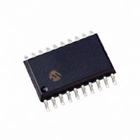
PIC16F785-I/SO Microchip Technology, PIC16F785-I/SO Datasheet - Page 23

PIC16F785-I/SO
Manufacturer Part Number
PIC16F785-I/SO
Description
IC PIC MCU FLASH 2KX14 20SOIC
Manufacturer
Microchip Technology
Series
PIC® 16Fr
Datasheets
1.PIC16F616T-ISL.pdf
(8 pages)
2.PIC16F785-ISS.pdf
(206 pages)
3.PIC16F785-ISS.pdf
(10 pages)
4.PIC16F785-ISS.pdf
(28 pages)
5.PIC16F785-IP.pdf
(178 pages)
Specifications of PIC16F785-I/SO
Program Memory Type
FLASH
Program Memory Size
3.5KB (2K x 14)
Package / Case
20-SOIC (7.5mm Width)
Core Processor
PIC
Core Size
8-Bit
Speed
20MHz
Peripherals
Brown-out Detect/Reset, POR, PWM, WDT
Number Of I /o
17
Eeprom Size
256 x 8
Ram Size
128 x 8
Voltage - Supply (vcc/vdd)
2 V ~ 5.5 V
Data Converters
A/D 14x10b
Oscillator Type
Internal
Operating Temperature
-40°C ~ 85°C
Processor Series
PIC16F
Core
PIC
Data Bus Width
8 bit
Data Ram Size
128 B
Interface Type
RS- 232/USB
Maximum Clock Frequency
20 MHz
Number Of Programmable I/os
17
Number Of Timers
3
Operating Supply Voltage
2 V to 5.5 V
Maximum Operating Temperature
+ 85 C
Mounting Style
SMD/SMT
3rd Party Development Tools
52715-96, 52716-328, 52717-734
Development Tools By Supplier
PG164130, DV164035, DV244005, DV164005, PG164120, ICE2000, DV164120, DM163029
Minimum Operating Temperature
- 40 C
On-chip Adc
14-ch x 10-bit
Lead Free Status / RoHS Status
Lead free / RoHS Compliant
For Use With
XLT20SO1-1 - SOCKET TRANS ICE 20DIP TO 20SOICXLT18SO-1 - SOCKET TRANSITION 18SOIC 300MILAC162060 - HEADER INTRFC MPLAB ICD2 20PINAC164039 - MODULE SKT PROMATE II 20DIP/SOIC
Connectivity
-
Lead Free Status / Rohs Status
Lead free / RoHS Compliant
Available stocks
Company
Part Number
Manufacturer
Quantity
Price
Part Number:
PIC16F785-I/SO
Manufacturer:
MICROCHIP/微芯
Quantity:
20 000
2.3
The Program Counter (PC) specifies the address of the
instruction to fetch for execution. The program counter
is 13 bits wide. The low byte is called the PCL register.
The PCL register readable and writable. The high byte
of the PC (PC<12:8>) is called the PCH register. This
register contains PC<12:8> bits which are not directly
readable or writable. All updates to the PCH register go
through the PCLATH register.
On any Reset, the PC is cleared. Figure 2-3 shows the
two situations for the loading of the PC. The upper
example in Figure 2-3 shows how the PC is loaded on
a write to PCL (PCLATH<4:0>
example in Figure 2-3 shows how the PC is loaded
during a CALL or GOTO instruction (PCLATH<4:3>
PCH).
2.3.1
Executing any instruction with the PCL register as the
destination
Counter PC<12:8> bits (PCH) to be replaced by the
contents of the PCLATH register. This allows the entire
contents of the program counter to be changed by first
writing the desired upper 5 bits to the PCLATH register.
When the lower 8 bits are then written to the PCL
register, all 13 bits of the program counter will change
to the values contained in the PCLATH register and
those being written to the PCL register.
A computed GOTO is accomplished by adding an offset
to the program counter (ADDWF PCL). Care should be
exercised when jumping into a look-up table or
program branch table (computed GOTO) by modifying
the PCL register. Assuming that PCLATH is set to the
table start address, if the table length is greater than
255 instructions, or if the lower 8 bits of the memory
address rolls over from 0xFF to 0x00 in the middle of
the table, then PCLATH must be incremented for each
address rollover that occurs between the table
beginning and the target location within the table.
For more information refer to Application Note
DS00556, “Implementing a Table Read” .
2.3.2
The CALL and GOTO instructions provide 11 bits of
address to allow branching within any 2K program
memory page. When doing a CALL or GOTO instruction,
the upper bit of the address is provided by PCLATH<3>
(page select bit). When doing a CALL or GOTO instruc-
tion the user must ensure that the page select bit is pro-
grammed so that the desired destination program
memory page is addressed. When the CALL instruction
(or interrupt) is executed, the entire 13-bit PC return
address is push ed onto the stack. Therefore, manipu-
lation of the PCLATH<3> bit is not required for the
RETURN or RETFIE instructions which pop the address
from the stack.
2004 Microchip Technology Inc.
PCL and PCLATH
MODIFYING PCL
PROGRAM MEMORY PAGING
simultaneously causes the
PCH). The lower
Program
Preliminary
FIGURE 2-3:
2.3.3
The PIC16F785 family has an 8-level x 13-bit wide
hardware stack (see Figure 2-1). The stack space is
not part of either program or data space and the stack
pointer is not readable or writable. The PC is PUSHed
onto the stack when a CALL instruction is executed or
an interrupt causes a branch. The stack is POPed in
the event of a RETURN,
instruction execution. PCLATH is not affected by a
PUSH or POP operation.
The stack operates as a circular buffer. This means that
after the stack has been PUSHed eight times, the ninth
PUSH overwrites the value that was stored from the
first PUSH. The tenth PUSH overwrites the second
PUSH (and so on).
PC
PC
Note 1: There are no Status bits to indicate stack
12
12 11 10
2
2: There are no instructions/mnemonics
5
PCH
PCLATH<4:3>
PCH
STACK
overflow or stack underflow conditions.
called push or pop . These are actions that
occur from the execution of the CALL,
RETURN, RETLW and RETFIE instruc-
tions or the vectoring to an interrupt
address.
PCLATH
PCLATH<4:0>
8
PCLATH
8
7
7
LOADING OF PC IN
DIFFERENT SITUATIONS
PCL
PCL
PIC16F785
RETLW or a RETFIE
11
8
DS41249A-page 21
INSTRUCTION WITH
0
0
OPCODE <10:0>
ALU RESULT
GOTO, CALL
DESTINATION
PCL AS


