R5F212H1SDSP#U0 Renesas Electronics America, R5F212H1SDSP#U0 Datasheet - Page 5
R5F212H1SDSP#U0
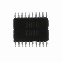
Manufacturer Part Number
R5F212H1SDSP#U0
Description
IC R8C/2H MCU FLASH 4K 20-SSOP
Manufacturer
Renesas Electronics America
Series
R8C/2x/2Hr
Datasheet
1.R5F212J0SNSPU0.pdf
(70 pages)
Specifications of R5F212H1SDSP#U0
Core Processor
R8C
Core Size
16/32-Bit
Speed
8MHz
Connectivity
LIN, SIO, UART/USART
Peripherals
POR, PWM, Voltage Detect, WDT
Number Of I /o
15
Program Memory Size
4KB (4K x 8)
Program Memory Type
FLASH
Ram Size
256 x 8
Voltage - Supply (vcc/vdd)
2.2 V ~ 5.5 V
Oscillator Type
Internal
Operating Temperature
-40°C ~ 85°C
Package / Case
20-SSOP
Lead Free Status / RoHS Status
Lead free / RoHS Compliant
Eeprom Size
-
Data Converters
-


R8C/2H Group, R8C/2J Group
Rev.1.00
REJ03B0217-0100
Table 1.2
NOTE:
CPU
Memory
Power Supply
Voltage
Detection
Comparator
I/O Ports
Clock
Interrupts
Watchdog Timer
Timer
Serial
Interface
LIN Module
Flash Memory
Operating Frequency/Supply
Voltage
Current consumption
Operating Ambient Temperature
Package
1. Specify the D version if D version functions are to be used.
Item
Mar 28, 2008
Specifications for R8C/2J Group
Central processing
unit
ROM, RAM
Voltage detection
circuit
Clock generation
circuits
Timer RA
Timer RB
Timer RE
Timer RF
UART0
Function
Page 3 of 65
R8C/Tiny series core
• Number of fundamental instructions: 89
• Minimum instruction execution time:
• Multiplier: 16 bits × 16 bits → 32 bits
• Multiply-accumulate instruction: 16 bits × 16 bits + 32 bits → 32 bits
• Operation mode: Single-chip mode (address space: 1 Mbyte)
Refer to Table 1.4 Product List for R8C/2J Group.
• Power-on reset
• Voltage detection 3
• 2 circuits (shared with voltage monitor 1 and voltage monitor 2)
• External reference voltage input is available
CMOS I/O ports: 12, selectable pull-up resistor
• 1 circuits: On-chip oscillator (high-speed, low-speed)
• Frequency divider circuit: Dividing selectable 1, 2, 4, 8, and 16
• Low power consumption modes:
• External: 3 sources, Internal: 14 sources, Software: 4 sources
• Priority levels: 7 levels
15 bits × 1 (with prescaler), reset start selectable
8 bits × 1 (with 8-bit prescaler)
8 bits × 1 (with 8-bit prescaler)
Not implemented
16 bits × 1 (with capture/compare register pin and compare register pin)
Clock synchronous serial I/O/UART × 1
Hardware LIN: 1 (timer RA, UART0)
• Programming and erasure voltage: VCC = 2.7 to 5.5 V
• Programming and erasure endurance: 100 times
• Program security: ROM code protect, ID code check
• Debug functions: On-chip debug, on-board flash rewrite function
System clock = 8 MHz (VCC = 2.7 to 5.5 V)
System clock = 4 MHz (VCC = 2.2 to 5.5 V)
5 mA (VCC = 5 V, system clock = 8 MHz)
23 µA (VCC = 3 V, wait mode (low-speed on-chip oscillator on))
0.7 µA (VCC = 3 V, stop mode, BGR trimming circuit disabled)
-20 to 85°C (N version)
-40 to 85°C (D version)
20-pin LSSOP
Timer mode (period timer), pulse output mode (output level inverted every
period), event counter mode, pulse width measurement mode, pulse period
measurement mode
Timer mode (period timer), programmable waveform generation mode (PWM
output), programmable one-shot generation mode, programmable wait one-
shot generation mode
Input capture mode, output compare mode
Package code: PLSP0020JB-A (previous code: 20P2F-A)
Standard operating mode (high-speed on-chip oscillator, low-speed on-chip
oscillator), wait mode, stop mode
125 ns (System clock = 8 MHz, VCC = 2.7 to 5.5 V)
250 ns (System clock = 4 MHz, VCC = 2.2 to 5.5 V)
(high-speed on-chip oscillator has a frequency adjustment function),
(1)
Specification
1. Overview
Related parts for R5F212H1SDSP#U0
Image
Part Number
Description
Manufacturer
Datasheet
Request
R

Part Number:
Description:
KIT STARTER FOR M16C/29
Manufacturer:
Renesas Electronics America
Datasheet:

Part Number:
Description:
KIT STARTER FOR R8C/2D
Manufacturer:
Renesas Electronics America
Datasheet:

Part Number:
Description:
R0K33062P STARTER KIT
Manufacturer:
Renesas Electronics America
Datasheet:

Part Number:
Description:
KIT STARTER FOR R8C/23 E8A
Manufacturer:
Renesas Electronics America
Datasheet:

Part Number:
Description:
KIT STARTER FOR R8C/25
Manufacturer:
Renesas Electronics America
Datasheet:

Part Number:
Description:
KIT STARTER H8S2456 SHARPE DSPLY
Manufacturer:
Renesas Electronics America
Datasheet:

Part Number:
Description:
KIT STARTER FOR R8C38C
Manufacturer:
Renesas Electronics America
Datasheet:

Part Number:
Description:
KIT STARTER FOR R8C35C
Manufacturer:
Renesas Electronics America
Datasheet:

Part Number:
Description:
KIT STARTER FOR R8CL3AC+LCD APPS
Manufacturer:
Renesas Electronics America
Datasheet:
Part Number:
Description:
KIT STARTER FOR RX610
Manufacturer:
Renesas Electronics America
Datasheet:

Part Number:
Description:
KIT STARTER FOR R32C/118
Manufacturer:
Renesas Electronics America
Datasheet:

Part Number:
Description:
KIT DEV RSK-R8C/26-29
Manufacturer:
Renesas Electronics America
Datasheet:

Part Number:
Description:
KIT STARTER FOR SH7124
Manufacturer:
Renesas Electronics America
Datasheet:

Part Number:
Description:
KIT STARTER FOR H8SX/1622
Manufacturer:
Renesas Electronics America
Datasheet:

Part Number:
Description:
KIT DEV FOR SH7203
Manufacturer:
Renesas Electronics America
Datasheet: