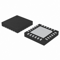
C8051F902-GM Silicon Laboratories Inc, C8051F902-GM Datasheet - Page 110

C8051F902-GM
Manufacturer Part Number
C8051F902-GM
Description
IC MCU 8BIT 8KB FLASH 24QFN
Manufacturer
Silicon Laboratories Inc
Series
C8051F9xxr
Specifications of C8051F902-GM
Program Memory Type
FLASH
Program Memory Size
8KB (8K x 8)
Package / Case
24-QFN
Core Processor
8051
Core Size
8-Bit
Speed
25MHz
Connectivity
SMBus (2-Wire/I²C), SPI, UART/USART
Peripherals
Brown-out Detect/Reset, POR, PWM, Temp Sensor, WDT
Number Of I /o
16
Ram Size
768 x 8
Voltage - Supply (vcc/vdd)
0.9 V ~ 3.6 V
Data Converters
A/D 15x10/12b
Oscillator Type
Internal
Operating Temperature
-40°C ~ 85°C
Processor Series
C8051F9x
Core
8051
Data Ram Size
768 B
Interface Type
UART
Maximum Clock Frequency
25 MHz
Number Of Timers
4
Operating Supply Voltage
0.9 V to 3.6 V
Maximum Operating Temperature
+ 85 C
Mounting Style
SMD/SMT
3rd Party Development Tools
PK51, CA51, A51, ULINK2
Development Tools By Supplier
C8051F912DK
Minimum Operating Temperature
- 40 C
On-chip Adc
12 bit
Package
24QFN EP
Device Core
8051
Family Name
C8051F90x
Maximum Speed
25 MHz
Data Bus Width
8 Bit
Number Of Programmable I/os
16
Lead Free Status / RoHS Status
Lead free / RoHS Compliant
Eeprom Size
-
Lead Free Status / Rohs Status
Lead free / RoHS Compliant
Other names
336-1848-5
- Current page: 110 of 318
- Download datasheet (3Mb)
C8051F91x-C8051F90x
9.2.1.3. Stack
A programmer's stack can be located anywhere in the 256-byte data memory. The stack area is
designated using the Stack Pointer (SP) SFR. The SP will point to the last location used. The next value
pushed on the stack is placed at SP+1 and then SP is incremented. A reset initializes the stack pointer to
location 0x07. Therefore, the first value pushed on the stack is placed at location 0x08, which is also the
first register (R0) of register bank 1. Thus, if more than one register bank is to be used, the SP should be
initialized to a location in the data memory not being used for data storage. The stack depth can extend up
to 256 bytes.
9.2.2. External RAM
There are 512 bytes of on-chip RAM mapped into the external data memory space. All of these address
locations may be accessed using the external move instruction (MOVX) and the data pointer (DPTR), or
using MOVX indirect addressing mode (such as @R1) in combination with the EMI0CN register.
110
Rev. 1.0
Related parts for C8051F902-GM
Image
Part Number
Description
Manufacturer
Datasheet
Request
R
Part Number:
Description:
SMD/C°/SINGLE-ENDED OUTPUT SILICON OSCILLATOR
Manufacturer:
Silicon Laboratories Inc
Part Number:
Description:
Manufacturer:
Silicon Laboratories Inc
Datasheet:
Part Number:
Description:
N/A N/A/SI4010 AES KEYFOB DEMO WITH LCD RX
Manufacturer:
Silicon Laboratories Inc
Datasheet:
Part Number:
Description:
N/A N/A/SI4010 SIMPLIFIED KEY FOB DEMO WITH LED RX
Manufacturer:
Silicon Laboratories Inc
Datasheet:
Part Number:
Description:
N/A/-40 TO 85 OC/EZLINK MODULE; F930/4432 HIGH BAND (REV E/B1)
Manufacturer:
Silicon Laboratories Inc
Part Number:
Description:
EZLink Module; F930/4432 Low Band (rev e/B1)
Manufacturer:
Silicon Laboratories Inc
Part Number:
Description:
I°/4460 10 DBM RADIO TEST CARD 434 MHZ
Manufacturer:
Silicon Laboratories Inc
Part Number:
Description:
I°/4461 14 DBM RADIO TEST CARD 868 MHZ
Manufacturer:
Silicon Laboratories Inc
Part Number:
Description:
I°/4463 20 DBM RFSWITCH RADIO TEST CARD 460 MHZ
Manufacturer:
Silicon Laboratories Inc
Part Number:
Description:
I°/4463 20 DBM RADIO TEST CARD 868 MHZ
Manufacturer:
Silicon Laboratories Inc
Part Number:
Description:
I°/4463 27 DBM RADIO TEST CARD 868 MHZ
Manufacturer:
Silicon Laboratories Inc
Part Number:
Description:
I°/4463 SKYWORKS 30 DBM RADIO TEST CARD 915 MHZ
Manufacturer:
Silicon Laboratories Inc
Part Number:
Description:
N/A N/A/-40 TO 85 OC/4463 RFMD 30 DBM RADIO TEST CARD 915 MHZ
Manufacturer:
Silicon Laboratories Inc
Part Number:
Description:
I°/4463 20 DBM RADIO TEST CARD 169 MHZ
Manufacturer:
Silicon Laboratories Inc


