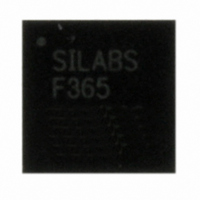
C8051F365-GM Silicon Laboratories Inc, C8051F365-GM Datasheet - Page 142

C8051F365-GM
Manufacturer Part Number
C8051F365-GM
Description
IC 8051 MCU 32K FLASH 28-QFN
Manufacturer
Silicon Laboratories Inc
Series
C8051F36xr
Specifications of C8051F365-GM
Program Memory Type
FLASH
Program Memory Size
32KB (32K x 8)
Package / Case
28-QFN
Core Processor
8051
Core Size
8-Bit
Speed
100MHz
Connectivity
SMBus (2-Wire/I²C), SPI, UART/USART
Peripherals
POR, PWM, Temp Sensor, WDT
Number Of I /o
25
Ram Size
1K x 8
Voltage - Supply (vcc/vdd)
3 V ~ 3.6 V
Oscillator Type
Internal
Operating Temperature
-40°C ~ 85°C
Processor Series
C8051F3x
Core
8051
Data Bus Width
8 bit
Data Ram Size
1 KB
Interface Type
I2C/SMBus/SPI/UART
Maximum Clock Frequency
100 MHz
Number Of Programmable I/os
25
Number Of Timers
4
Maximum Operating Temperature
+ 85 C
Mounting Style
SMD/SMT
3rd Party Development Tools
KSK-SL-TOOLSTICK, PK51, CA51, A51, ULINK2
Development Tools By Supplier
C8051F360DK
Minimum Operating Temperature
- 40 C
Package
28QFN
Device Core
8051
Family Name
C8051F36x
Maximum Speed
100 MHz
Operating Supply Voltage
3.3 V
Lead Free Status / RoHS Status
Lead free / RoHS Compliant
For Use With
770-1006 - ISP 4PORT FOR SILABS C8051F MCU336-1410 - KIT DEV FOR C8051F360 FAMILY
Eeprom Size
-
Data Converters
-
Lead Free Status / Rohs Status
Lead free / RoHS Compliant
Other names
336-1647
Available stocks
Company
Part Number
Manufacturer
Quantity
Price
Part Number:
C8051F365-GM
Manufacturer:
SILICON LABS/芯科
Quantity:
20 000
- Current page: 142 of 288
- Download datasheet (3Mb)
C8051F360/1/2/3/4/5/6/7/8/9
142
Bits 7–2: UNUSED. Read = 000000b, Write = don't care.
Bit 1:
Bit 0:
SFR Page:
SFR Address:
Bits 7–0: FLKEY: Flash Lock and Key Register
SFR Page:
SFR Address:
R/W
R/W
Bit7
Bit7
–
PSEE: Program Store Erase Enable.
Setting this bit allows an entire page of the Flash program memory to be erased provided
the PSWE bit is also set. After setting this bit, a write to Flash memory using the MOVX
instruction will erase the entire page that contains the location addressed by the MOVX
instruction. The value of the data byte written does not matter. Note: The Flash page con-
taining the Read Lock Byte and Write/Erase Lock Byte cannot be erased by software.
0: Flash program memory erasure disabled.
1: Flash program memory erasure enabled.
PSWE: Program Store Write Enable.
Setting this bit allows writing a byte of data to the Flash program memory using the MOVX
write instruction. The location must be erased prior to writing data.
0: Write to Flash program memory disabled. MOVX write operations target External RAM.
1: Write to Flash program memory enabled. MOVX write operations target Flash memory.
Write:
This register provides a lock and key function for Flash erasures and writes. Flash writes
and erases are enabled by writing 0xA5 followed by 0xF1 to the FLKEY register. Flash
writes and erases are automatically disabled after the next write or erase is complete. If any
writes to FLKEY are performed incorrectly, or if a Flash write or erase operation is attempted
while these operations are disabled, the Flash will be permanently locked from writes or era-
sures until the next device reset. If an application never writes to Flash, it can intentionally
lock the Flash by writing a non-0xA5 value to FLKEY from software.
Read:
When read, bits 1-0 indicate the current Flash lock state.
00: Flash is write/erase locked.
01: The first key code has been written (0xA5).
10: Flash is unlocked (writes/erases allowed).
11: Flash writes/erases disabled until the next reset.
SFR Definition 13.1.
0
0x8F
0
0xB7
R/W
R/W
Bit6
Bit6
–
SFR Definition 13.2. FLKEY: Flash Lock and Key
R/W
Bit5
R/W
Bit5
–
PSCTL: Program Store Read/Write Control
R/W
Bit4
R/W
Bit4
–
Rev. 1.0
R/W
Bit3
R/W
Bit3
–
R/W
Bit2
R/W
Bit2
–
PSEE
R/W
R/W
Bit1
Bit1
PSWE
R/W
Bit0
R/W
Bit0
00000000
Reset Value
00000000
Reset Value
Related parts for C8051F365-GM
Image
Part Number
Description
Manufacturer
Datasheet
Request
R
Part Number:
Description:
SMD/C°/SINGLE-ENDED OUTPUT SILICON OSCILLATOR
Manufacturer:
Silicon Laboratories Inc
Part Number:
Description:
Manufacturer:
Silicon Laboratories Inc
Datasheet:
Part Number:
Description:
N/A N/A/SI4010 AES KEYFOB DEMO WITH LCD RX
Manufacturer:
Silicon Laboratories Inc
Datasheet:
Part Number:
Description:
N/A N/A/SI4010 SIMPLIFIED KEY FOB DEMO WITH LED RX
Manufacturer:
Silicon Laboratories Inc
Datasheet:
Part Number:
Description:
N/A/-40 TO 85 OC/EZLINK MODULE; F930/4432 HIGH BAND (REV E/B1)
Manufacturer:
Silicon Laboratories Inc
Part Number:
Description:
EZLink Module; F930/4432 Low Band (rev e/B1)
Manufacturer:
Silicon Laboratories Inc
Part Number:
Description:
I°/4460 10 DBM RADIO TEST CARD 434 MHZ
Manufacturer:
Silicon Laboratories Inc
Part Number:
Description:
I°/4461 14 DBM RADIO TEST CARD 868 MHZ
Manufacturer:
Silicon Laboratories Inc
Part Number:
Description:
I°/4463 20 DBM RFSWITCH RADIO TEST CARD 460 MHZ
Manufacturer:
Silicon Laboratories Inc
Part Number:
Description:
I°/4463 20 DBM RADIO TEST CARD 868 MHZ
Manufacturer:
Silicon Laboratories Inc
Part Number:
Description:
I°/4463 27 DBM RADIO TEST CARD 868 MHZ
Manufacturer:
Silicon Laboratories Inc
Part Number:
Description:
I°/4463 SKYWORKS 30 DBM RADIO TEST CARD 915 MHZ
Manufacturer:
Silicon Laboratories Inc
Part Number:
Description:
N/A N/A/-40 TO 85 OC/4463 RFMD 30 DBM RADIO TEST CARD 915 MHZ
Manufacturer:
Silicon Laboratories Inc
Part Number:
Description:
I°/4463 20 DBM RADIO TEST CARD 169 MHZ
Manufacturer:
Silicon Laboratories Inc


