DF2214BQ16V Renesas Electronics America, DF2214BQ16V Datasheet - Page 52
DF2214BQ16V
Manufacturer Part Number
DF2214BQ16V
Description
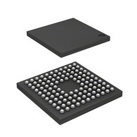
IC H8S/2214 MCU FLASH 112-TFBGA
Manufacturer
Renesas Electronics America
Series
H8® H8S/2200r
Datasheets
1.HS2214ECB62H.pdf
(938 pages)
2.HEWH8E10A.pdf
(19 pages)
3.D12312SVTE25V.pdf
(341 pages)
Specifications of DF2214BQ16V
Core Processor
H8S/2000
Core Size
16-Bit
Speed
16MHz
Connectivity
SCI
Peripherals
DMA, POR, PWM, WDT
Number Of I /o
72
Program Memory Size
128KB (128K x 8)
Program Memory Type
FLASH
Ram Size
12K x 8
Voltage - Supply (vcc/vdd)
2.7 V ~ 3.6 V
Data Converters
D/A 1x8b
Oscillator Type
Internal
Operating Temperature
-20°C ~ 75°C
Package / Case
112-TFBGA
For Use With
HS0005KCU11H - EMULATOR E10A-USB H8S(X),SH2(A)3DK2218 - DEV EVAL KIT H8S/2218
Lead Free Status / RoHS Status
Lead free / RoHS Compliant
Eeprom Size
-
Available stocks
Company
Part Number
Manufacturer
Quantity
Price
Company:

Part Number:
DF2214BQ16V
Manufacturer:
Renesas Electronics America
Quantity:
10 000


Figure 10.52 Contention between Overflow and Counter Clearing ............................................. 435
Figure 10.53 Contention between TCNT Write and Overflow .................................................... 436
Section 11 Watchdog Timer (WDT)
Figure 11.1 Block Diagram of WDT.......................................................................................... 438
Figure 11.2 Format of Data Written to TCNT and TCSR (Example of WDT0) ........................ 444
Figure 11.3 Format of Data Written to RSTCSR (Example of WDT0) ..................................... 445
Figure 11.4 Operation in Watchdog Timer Mode ...................................................................... 446
Figure 11.5 Operation in Interval Timer Mode .......................................................................... 447
Figure 11.6 Timing of OVF Setting ........................................................................................... 448
Figure 11.7 Timing of WOVF Setting........................................................................................ 449
Figure 11.8 Contention between TCNT Write and Increment.................................................... 450
Section 12 Serial Communication Interface (SCI)
Figure 12.1 Block Diagram of SCI0........................................................................................... 455
Figure 12.2 Block Diagram of SCI1 and SCI2 ........................................................................... 456
Figure 12.3 Examples of Base Clock when Average Transfer Rate Is Selected (1)................... 484
Figure 12.4 Examples of Base Clock when Average Transfer Rate Is Selected (2)................... 485
Figure 12.5 Data Format in Asynchronous Communication
Figure 12.6 Relation between Output Clock and Transfer Data Phase (Asynchronous Mode). 492
Figure 12.7 Sample SCI Initialization Flowchart ....................................................................... 493
Figure 12.8 Sample Serial Transmission Flowchart ................................................................... 494
Figure 12.9 Example of Operation in Transmission in Asynchronous Mode
Figure 12.10 Sample Serial Reception Data Flowchart (1) .......................................................... 497
Figure 12.11 Sample Serial Reception Data Flowchart (2) .......................................................... 498
Figure 12.12 Example of SCI Operation in Reception
Figure 12.13 Example of Inter-Processor Communication Using Multiprocessor Format
Figure 12.14 Sample Multiprocessor Serial Transmission Flowchart .......................................... 503
Figure 12.15 Example of SCI Operation in Transmission
Figure 12.16 Sample Multiprocessor Serial Reception Flowchart (1).......................................... 506
Figure 12.17 Sample Multiprocessor Serial Reception Flowchart (2).......................................... 507
Figure 12.18 Example of SCI Operation in Reception
Figure 12.19 Data Format in Synchronous Communication ........................................................ 509
Figure 12.20 Sample SCI Initialization Flowchart ....................................................................... 511
Figure 12.21 Sample Serial Transmission Flowchart ................................................................... 512
Rev.4.00 Sep. 18, 2008 Page l of lx
REJ09B0189-0400
(Example with 8-Bit Data, Parity, Two Stop Bits).................................................. 490
(Example with 8-Bit Data, Parity, One Stop Bit) .................................................... 496
(Example with 8-Bit Data, Parity, One Stop Bit) .................................................... 500
(Transmission of Data H'AA to Receiving Station A) ............................................ 502
(Example with 8-Bit Data, Multiprocessor Bit, One Stop Bit)................................ 505
(Example with 8-Bit Data, Multiprocessor Bit, One Stop Bit)................................ 508
Related parts for DF2214BQ16V
Image
Part Number
Description
Manufacturer
Datasheet
Request
R

Part Number:
Description:
CONN SOCKET 2POS 7.92MM WHITE
Manufacturer:
Hirose Electric Co Ltd
Datasheet:

Part Number:
Description:
CONN SOCKET 4POS 7.92MM WHITE
Manufacturer:
Hirose Electric Co Ltd
Datasheet:

Part Number:
Description:
CONN SOCKET 5POS 7.92MM WHITE
Manufacturer:
Hirose Electric Co Ltd
Datasheet:

Part Number:
Description:
CONN SOCKET 3POS 7.92MM WHITE
Manufacturer:
Hirose Electric Co Ltd
Datasheet:
Part Number:
Description:
CONN SOCKET 5POS 7.92MM WHITE
Manufacturer:
Hirose Electric Co Ltd
Datasheet:

Part Number:
Description:
CONN SOCKET 2POS 7.92MM WHITE
Manufacturer:
Hirose Electric Co Ltd
Datasheet:
Part Number:
Description:
CONN SOCKET 3POS 7.92MM WHITE
Manufacturer:
Hirose Electric Co Ltd
Datasheet:
Part Number:
Description:
CONN SOCKET 4POS 7.92MM WHITE
Manufacturer:
Hirose Electric Co Ltd
Datasheet:

Part Number:
Description:
CONN HEADER 2POS 7.92MM R/A TIN
Manufacturer:
Hirose Electric Co Ltd
Datasheet:

Part Number:
Description:
CONN HEADER 4POS 7.92MM R/A TIN
Manufacturer:
Hirose Electric Co Ltd
Datasheet:

Part Number:
Description:
KIT STARTER FOR M16C/29
Manufacturer:
Renesas Electronics America
Datasheet:

Part Number:
Description:
KIT STARTER FOR R8C/2D
Manufacturer:
Renesas Electronics America
Datasheet:

Part Number:
Description:
R0K33062P STARTER KIT
Manufacturer:
Renesas Electronics America
Datasheet:

Part Number:
Description:
KIT STARTER FOR R8C/23 E8A
Manufacturer:
Renesas Electronics America
Datasheet:

Part Number:
Description:
KIT STARTER FOR R8C/25
Manufacturer:
Renesas Electronics America
Datasheet: