M30879FKBGP#U5 Renesas Electronics America, M30879FKBGP#U5 Datasheet - Page 243
M30879FKBGP#U5
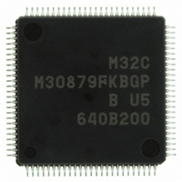
Manufacturer Part Number
M30879FKBGP#U5
Description
IC M32C/87 MCU FLASH 100LQFP
Manufacturer
Renesas Electronics America
Series
M16C™ M32C/80r
Datasheet
1.M3087BFLGPU3.pdf
(629 pages)
Specifications of M30879FKBGP#U5
Core Processor
M32C/80
Core Size
16/32-Bit
Speed
32MHz
Connectivity
EBI/EMI, I²C, IEBus, IrDA, SIO, UART/USART
Peripherals
DMA, POR, PWM, WDT
Number Of I /o
85
Program Memory Size
768KB (768K x 8)
Program Memory Type
FLASH
Ram Size
48K x 8
Voltage - Supply (vcc/vdd)
3 V ~ 5.5 V
Data Converters
A/D 26x10b; D/A 2x8b
Oscillator Type
Internal
Operating Temperature
-20°C ~ 85°C
Package / Case
100-LQFP
For Use With
R0K330879S001BE - KIT DEV RSK M32C/87R0K330879S000BE - KIT DEV RSK M32C/87
Lead Free Status / RoHS Status
Lead free / RoHS Compliant
Eeprom Size
-
Available stocks
Company
Part Number
Manufacturer
Quantity
Price

Part Number:
M30879FKBGP#U5M30879FKBGP#U3
Manufacturer:
Renesas Electronics America
Quantity:
10 000


M32C/87 Group (M32C/87, M32C/87A, M32C/87B)
REJ09B0180-0151 Rev.1.51 Jul 31, 2008
Page 219 of 587
Figure 17.5
UARTi Special Mode Register 3 (i = 0 to 4)
b7 b6 b5 b4
NOTES:
1. These bits are used in special mode 2.
2. When the SS pin is set to 1, set the CRD bit in the UiC0 register to 1 ( CTS function disabled).
3. The ERR bit is set to 0 by a program. Writing a 1 has no effect.
4. Digital delay is added to a SDAi output using bits DL2 to DL0 in I
5. When the external clock is selected, SDAi output is delayed by approximately 100 ns in addition.
b3
b2
U0SMR3 to U4SMR3 Registers
b1
b0
Bit Symbol
CKPH
NODC
DINC
SSE
ERR
Symbol
U0SMR3 to U2SMR3
U3SMR3, U4SMR3
DL0
DL1
DL2
SS function enable bit
Clock phase set bit
Serial input pin set bit
Clock output select bit
Mode error flag
SDAi digital delay set bits
Bit Name
(1)
(1)
(1)
(1)
(4, 5)
Address
0365h, 02E5h, 0335h
0325h, 02F5h
2
C mode. Set them to 000b (no delay) in other than I
0: SS function disabled
1: SS function enabled
0: No Clock delay
1: Clock delay
0: Pins TXDi and RXDi selected (master mode)
1: Pins STXDi and SRXDi selected (slave mode)
0: CLKi is CMOS output
1: CLKi is N-channel open drain output
0: No mode error
1: Mode error occurred
SDAi output is delayed by the following cycles.
b7 b6 b5
0 0 0: No delay
0 0 1: 1-to-2 cycles of BRG count source
0 1 0: 2-to-3 cycles of BRG count source
0 1 1: 3-to-4 cycles of BRG count source
1 0 0: 4-to-5 cycles of BRG count source
1 0 1: 5-to-6 cycles of BRG count source
1 1 0: 6-to-7 cycles of BRG count source
1 1 1: 7-to-8 cycles of BRG count source
17. Serial Interfaces (UART0 to UART4)
Function
(2)
(3)
After Reset
00h
00h
2
C mode.
RW
RW
RW
RW
RW
RW
RW
RW
RW
Related parts for M30879FKBGP#U5
Image
Part Number
Description
Manufacturer
Datasheet
Request
R

Part Number:
Description:
KIT STARTER FOR M16C/29
Manufacturer:
Renesas Electronics America
Datasheet:

Part Number:
Description:
KIT STARTER FOR R8C/2D
Manufacturer:
Renesas Electronics America
Datasheet:

Part Number:
Description:
R0K33062P STARTER KIT
Manufacturer:
Renesas Electronics America
Datasheet:

Part Number:
Description:
KIT STARTER FOR R8C/23 E8A
Manufacturer:
Renesas Electronics America
Datasheet:

Part Number:
Description:
KIT STARTER FOR R8C/25
Manufacturer:
Renesas Electronics America
Datasheet:

Part Number:
Description:
KIT STARTER H8S2456 SHARPE DSPLY
Manufacturer:
Renesas Electronics America
Datasheet:

Part Number:
Description:
KIT STARTER FOR R8C38C
Manufacturer:
Renesas Electronics America
Datasheet:

Part Number:
Description:
KIT STARTER FOR R8C35C
Manufacturer:
Renesas Electronics America
Datasheet:

Part Number:
Description:
KIT STARTER FOR R8CL3AC+LCD APPS
Manufacturer:
Renesas Electronics America
Datasheet:
Part Number:
Description:
KIT STARTER FOR RX610
Manufacturer:
Renesas Electronics America
Datasheet:

Part Number:
Description:
KIT STARTER FOR R32C/118
Manufacturer:
Renesas Electronics America
Datasheet:

Part Number:
Description:
KIT DEV RSK-R8C/26-29
Manufacturer:
Renesas Electronics America
Datasheet:

Part Number:
Description:
KIT STARTER FOR SH7124
Manufacturer:
Renesas Electronics America
Datasheet:

Part Number:
Description:
KIT STARTER FOR H8SX/1622
Manufacturer:
Renesas Electronics America
Datasheet:

Part Number:
Description:
KIT DEV FOR SH7203
Manufacturer:
Renesas Electronics America
Datasheet: