M30879FKBGP#U5 Renesas Electronics America, M30879FKBGP#U5 Datasheet - Page 248
M30879FKBGP#U5
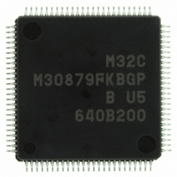
Manufacturer Part Number
M30879FKBGP#U5
Description
IC M32C/87 MCU FLASH 100LQFP
Manufacturer
Renesas Electronics America
Series
M16C™ M32C/80r
Datasheet
1.M3087BFLGPU3.pdf
(629 pages)
Specifications of M30879FKBGP#U5
Core Processor
M32C/80
Core Size
16/32-Bit
Speed
32MHz
Connectivity
EBI/EMI, I²C, IEBus, IrDA, SIO, UART/USART
Peripherals
DMA, POR, PWM, WDT
Number Of I /o
85
Program Memory Size
768KB (768K x 8)
Program Memory Type
FLASH
Ram Size
48K x 8
Voltage - Supply (vcc/vdd)
3 V ~ 5.5 V
Data Converters
A/D 26x10b; D/A 2x8b
Oscillator Type
Internal
Operating Temperature
-20°C ~ 85°C
Package / Case
100-LQFP
For Use With
R0K330879S001BE - KIT DEV RSK M32C/87R0K330879S000BE - KIT DEV RSK M32C/87
Lead Free Status / RoHS Status
Lead free / RoHS Compliant
Eeprom Size
-
Available stocks
Company
Part Number
Manufacturer
Quantity
Price

Part Number:
M30879FKBGP#U5M30879FKBGP#U3
Manufacturer:
Renesas Electronics America
Quantity:
10 000


M32C/87 Group (M32C/87, M32C/87A, M32C/87B)
REJ09B0180-0151 Rev.1.51 Jul 31, 2008
Page 224 of 587
Figure 17.10
UARTi Transmit Buffer Register
UARTi Receive Buffer Register (i = 0 to 4)
b15
b15
NOTE:
NOTES:
1. Read-modify-write instructions cannot be used to set the UiTB register. Refer to Usage Notes for details.
1. Only a 0 can be written to the ABT bit.
2. When bits SMD2 to SMD0 in the UiMR register are set to 000b (serial interface disabled) or the RE bit in the UiC1 register is set to
3. Bits FER, PER and SUM are disabled when bits SMD2 to SMD0 in the UiMR register are set to 001b (clock synchronous mode)
0 (receive operation disabled), bits OER, FER, PER and SUM become 0.
When all of bits OER, FER and PER become 0, the SUM bit also becomes 0.
Bits FER and PER become 0 by reading the low-order byte in the UiRB register.
or 010b (I
b8
b8
b7
b7
U0TB to U4TB Registers, U0RB to U4RB Registers
2
C mode). A read from these bits returns undefined value.
b0
b0
Bit Symbol
Bit Symbol
(b15-b9)
(b10-b9)
(b7-b0)
(b7-b0)
OER
SUM
FER
PER
ABT
(b8)
(b8)
Symbol
U0TB to U2TB
U3TB, U4TB
Symbol
U0RB to U2RB
U3RB, U4RB
−
−
−
−
−
−
Transmit data (D7 to D0)
Transmit data (D8)
Unimplemented.
Write 0. Read as undefined value.
Unimplemented.
Write 0. Read as undefined value.
Arbitration lost detect flag
Overrun error flag
Framing error flag
Parity error flag
Error sum flag
(1)
Bit Name
(i = 0 to 4)
(2, 3)
Address
Address
036Bh - 036Ah, 02EBh - 02EAh, 033Bh - 033Ah
032Bh - 032Ah, 02FBh - 02FAh
036Fh - 036Eh, 02EFh - 02EEh, 033Fh - 033Eh
032Fh - 032Eh, 02FFh - 02FEh
−
−
(2, 3)
(2)
(2, 3)
(1)
Received data (D7 to D0)
Received data (D8)
0: Not detected (won)
1: Detected (lost)
0: No overrun error
1: Overrun error
0: No framing error
1: Framing error
0: No parity error
1: Parity error
0 No error occurred
1: Error occurred
Function
17. Serial Interfaces (UART0 to UART4)
Function
After Reset
Undefined
Undefined
After Reset
Undefined
Undefined
WO
WO
RW
RW
RW
RO
RO
RO
RO
RO
RO
−
−
Related parts for M30879FKBGP#U5
Image
Part Number
Description
Manufacturer
Datasheet
Request
R

Part Number:
Description:
KIT STARTER FOR M16C/29
Manufacturer:
Renesas Electronics America
Datasheet:

Part Number:
Description:
KIT STARTER FOR R8C/2D
Manufacturer:
Renesas Electronics America
Datasheet:

Part Number:
Description:
R0K33062P STARTER KIT
Manufacturer:
Renesas Electronics America
Datasheet:

Part Number:
Description:
KIT STARTER FOR R8C/23 E8A
Manufacturer:
Renesas Electronics America
Datasheet:

Part Number:
Description:
KIT STARTER FOR R8C/25
Manufacturer:
Renesas Electronics America
Datasheet:

Part Number:
Description:
KIT STARTER H8S2456 SHARPE DSPLY
Manufacturer:
Renesas Electronics America
Datasheet:

Part Number:
Description:
KIT STARTER FOR R8C38C
Manufacturer:
Renesas Electronics America
Datasheet:

Part Number:
Description:
KIT STARTER FOR R8C35C
Manufacturer:
Renesas Electronics America
Datasheet:

Part Number:
Description:
KIT STARTER FOR R8CL3AC+LCD APPS
Manufacturer:
Renesas Electronics America
Datasheet:
Part Number:
Description:
KIT STARTER FOR RX610
Manufacturer:
Renesas Electronics America
Datasheet:

Part Number:
Description:
KIT STARTER FOR R32C/118
Manufacturer:
Renesas Electronics America
Datasheet:

Part Number:
Description:
KIT DEV RSK-R8C/26-29
Manufacturer:
Renesas Electronics America
Datasheet:

Part Number:
Description:
KIT STARTER FOR SH7124
Manufacturer:
Renesas Electronics America
Datasheet:

Part Number:
Description:
KIT STARTER FOR H8SX/1622
Manufacturer:
Renesas Electronics America
Datasheet:

Part Number:
Description:
KIT DEV FOR SH7203
Manufacturer:
Renesas Electronics America
Datasheet: