MC68332GCEH20 Freescale Semiconductor, MC68332GCEH20 Datasheet - Page 182
MC68332GCEH20
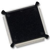
Manufacturer Part Number
MC68332GCEH20
Description
IC MCU 32BIT 20MHZ 132-PQFP
Manufacturer
Freescale Semiconductor
Series
M683xxr
Specifications of MC68332GCEH20
Core Processor
CPU32
Core Size
32-Bit
Speed
20MHz
Connectivity
EBI/EMI, SCI, SPI, UART/USART
Peripherals
POR, PWM, WDT
Number Of I /o
15
Program Memory Type
ROMless
Ram Size
2K x 8
Voltage - Supply (vcc/vdd)
4.5 V ~ 5.5 V
Oscillator Type
Internal
Operating Temperature
-40°C ~ 85°C
Package / Case
132-QFP
Controller Family/series
68K
No. Of I/o's
15
Ram Memory Size
2KB
Cpu Speed
20MHz
No. Of Timers
1
Embedded Interface Type
QSPI, SCI, UART
Digital Ic Case Style
PQFP
Rohs Compliant
Yes
Data Bus Width
32 bit
Data Ram Size
2 KB
Interface Type
QSPI, SCI, UART
Maximum Clock Frequency
20 MHz
Number Of Programmable I/os
15
Number Of Timers
16
Maximum Operating Temperature
+ 85 C
Mounting Style
SMD/SMT
Minimum Operating Temperature
- 40 C
Lead Free Status / RoHS Status
Lead free / RoHS Compliant
Eeprom Size
-
Program Memory Size
-
Data Converters
-
Lead Free Status / Rohs Status
Details
Available stocks
Company
Part Number
Manufacturer
Quantity
Price
Company:

Part Number:
MC68332GCEH20
Manufacturer:
Freescale Semiconductor
Quantity:
10 000
Part Number:
MC68332GCEH20
Manufacturer:
FREESCALE
Quantity:
20 000


A-8
10. When V
Notes for Tables A–5 and A–5a:
1. Applies to:
2. Input-Only Pins: EXTAL, TSTME/TSC, BKPT, T2CLK, RXD
3. Does not apply to HALT and RESET because they are open drain pins. Does not apply to Port QS [7:0] (TXD,
4. Current measured with system clock frequency of 16.78 MHz, all modules active.
5. Use of an active pulldown device is recommended.
6. Total operating current is the sum of the appropriate I
7.
8. Power dissipation measured at specified system clock frequency, all modules active. Power dissipation can be
9. This parameter is periodically sampled rather than 100% tested.
the V
ification. System noise on the V
Output-Only Pins: CSBOOT, BG/CS, CLKOUT, FREEZE/QUOT, IPIPE
Input/Output Pins:
PCS[3:1],ÊPCS0/SS, SCK, MOSI, MISO) in wired-OR mode.
rents for device modules powered by V
Volt. The RAM array cannot be accessed while the module is in standby mode.
calculated using the expression:
I
DD
includes supply currents for all device modules powered by V
STBY
Port E [7:4] — SIZ[1:0], AS, DS
Port F [7:0] — IRQ[7:1], MODCLK
Port QS [7:0] — TXD, PCS[3:1],ÊPCS0/SS, SCK, MOSI, MISO
TPUCH[15:0], T2CLK
BKPT/DSCLK, IFETCH, RESET, RXD, TSTME/TSC
EXTAL (when PLL enabled)
Group 1:
Group 2:
Group 3:
Group 4:
The RAM module will not switch into standby mode as long as V
DD
and V
is transitioning during power-up or power down sequence, and V
DD
P
pins, which causes standby current to increase toward the maximum transient condition spec-
D
DATA[15:0], IFETCH, TPUCH[15:0]
Port C [6:0] — ADDR[22:19]/CS[9:6], FC[2:0]/CS[5:3]
Port E [7:0] — SIZ[1:0], AS, DS, AVEC, RMC, DSACK[1:0]
Port F [&:0] — IRQ[7:1], MODCLK
Port QS [7:3] — TXD, PCS[3:1], PCS0/SS
ADDR23/CS10/ECLK, ADDR[18:0], R/W, BERR, BR/CS0, BGACK/CS2
HALT, RESET
MISO, MOSI, SCK
Maximum V
Freescale Semiconductor, Inc.
For More Information On This Product,
DD
ELECTRICAL CHARACTERISTICS
and V
DD
Go to: www.freescale.com
(I
DDE
DD
STBY
+ I
and V
DDSYN
pins can contribute to this condition.
DDI
+ I
pins.
DD
SB
, I
)
DDSYN
, and I
DDE
SB
and V
SB
does not exceed V
values. I
SB
DDI
is applied, current flows between
pins.
DD
values include supply cur-
USER’S MANUAL
DD
by more than 0.5
MC68332
Related parts for MC68332GCEH20
Image
Part Number
Description
Manufacturer
Datasheet
Request
R

Part Number:
Description:
Manufacturer:
Freescale Semiconductor, Inc
Datasheet:
Part Number:
Description:
Manufacturer:
Freescale Semiconductor, Inc
Datasheet:
Part Number:
Description:
Manufacturer:
Freescale Semiconductor, Inc
Datasheet:
Part Number:
Description:
Manufacturer:
Freescale Semiconductor, Inc
Datasheet:
Part Number:
Description:
Manufacturer:
Freescale Semiconductor, Inc
Datasheet:
Part Number:
Description:
Manufacturer:
Freescale Semiconductor, Inc
Datasheet:
Part Number:
Description:
Manufacturer:
Freescale Semiconductor, Inc
Datasheet:
Part Number:
Description:
Manufacturer:
Freescale Semiconductor, Inc
Datasheet:
Part Number:
Description:
Manufacturer:
Freescale Semiconductor, Inc
Datasheet:
Part Number:
Description:
Manufacturer:
Freescale Semiconductor, Inc
Datasheet:
Part Number:
Description:
Manufacturer:
Freescale Semiconductor, Inc
Datasheet:
Part Number:
Description:
Manufacturer:
Freescale Semiconductor, Inc
Datasheet:
Part Number:
Description:
Manufacturer:
Freescale Semiconductor, Inc
Datasheet:
Part Number:
Description:
Manufacturer:
Freescale Semiconductor, Inc
Datasheet:
Part Number:
Description:
Manufacturer:
Freescale Semiconductor, Inc
Datasheet: