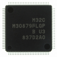
M30879FLGP#U3 Renesas Electronics America, M30879FLGP#U3 Datasheet - Page 400

M30879FLGP#U3
Manufacturer Part Number
M30879FLGP#U3
Description
IC M32C/87 MCU FLASH 100LQFP
Manufacturer
Renesas Electronics America
Series
M16C™ M32C/80r
Specifications of M30879FLGP#U3
Core Size
16/32-Bit
Program Memory Size
1MB (1M x 8)
Core Processor
M32C/80
Speed
32MHz
Connectivity
CAN, EBI/EMI, I²C, IEBus, IrDA, SIO, UART/USART
Peripherals
DMA, POR, PWM, WDT
Number Of I /o
85
Program Memory Type
FLASH
Ram Size
48K x 8
Voltage - Supply (vcc/vdd)
3 V ~ 5.5 V
Data Converters
A/D 26x10b; D/A 2x8b
Oscillator Type
Internal
Operating Temperature
-40°C ~ 85°C
Package / Case
100-LQFP
Controller Family/series
M32C
No. Of I/o's
85
Ram Memory Size
48KB
Cpu Speed
32MHz
No. Of Timers
2
Digital Ic Case Style
LQFP
Embedded Interface Type
CAN, I2C, UART
Rohs Compliant
Yes
Lead Free Status / RoHS Status
Lead free / RoHS Compliant
For Use With
R0K330879S001BE - KIT DEV RSK M32C/87R0K330879S000BE - KIT DEV RSK M32C/87
Eeprom Size
-
Lead Free Status / RoHS Status
Lead free / RoHS Compliant, Lead free / RoHS Compliant
Available stocks
Company
Part Number
Manufacturer
Quantity
Price
Part Number:
M30879FLGP#U3M30879FLGP#U5
Manufacturer:
Renesas Electronics America
Quantity:
10 000
- Current page: 400 of 629
- Download datasheet (16Mb)
M32C/87 Group (M32C/87, M32C/87A, M32C/87B) 22. Intelligent I/O (Group 0 and 1 Communication Function)
REJ09B0180-0151 Rev.1.51 Jul 31, 2008
Page 376 of 587
Figure 22.44
Group i Data Comparison Register j (i=0,1; j=0 to 3)
Group i Data Mask Register j (i=0,1; j=0,1)
Group i Transmit CRC Code Register (i=0,1)
Group i Receive CRC Code Register (i=0,1)
b15
b15
b7
b7
NOTE:
NOTES:
NOTES:
1. Set the GiMSK0 register to use the GiCMP0 register.
1. This register becomes the initial value selected by the CRCV bit in the GiEMR register when the TE bit in the GiCR register
2. Transmit CRC calculation is performed when each one bit of data is transmitted while the TCRCE bit in the GiETC register is set to
1. This register becomes the initial value selected by the CRCV bit in the GiEMR register when the RCRCE bit in the GiERC
2. This register is initialized before receive operation starts.
3. Receive CRC calculation is performed when each one bit of data is received while the RCRCE bit in the GiERC register is set to
Set the GiMSK1 register to use the GiCMP1 register.
1 (used).
is set to 0 (transmit operation disabled).
register is set to 0 (not used). If the ACRC bit in the GiEMRj (j = 0 to 3) register is set to 1 (initialized), this register is initialized
when the received data is matched the data in the GiCMPj register.
1 (used).
b8
b8
b7
b7
G0CMP0 to G0CMP3, G1CMP0 to G1CMP3 Registers, G0MSK0 and G0MSK1
Registers, G1MSK0 and G1MSK1 Registers, G0TCRC and G1TCRC Registers,
G0RCRC and G1RCRC Registers
b0
b0
b0
b0
Data to be compared
Masked data for received data
Write 1 to the bit which is not compared
Result of the transmit CRC calculation
Result of the receive CRC calculation
Symbol
G0CMP0 to G0CMP3
G1CMP0 to G1CMP3
Symbol
G0MSK0, G0MSK1
G1MSK0, G1MSK1
Symbol
G0TCRC, G1TCRC
Symbol
G0RCRC, G1RCRC
Function
Function
(1)(2)(3)
(1)(2)
Address
00F0h, 00F1h, 00F2h, 00F3h
0130h, 0131h, 0132h, 0133h
Address
00F4h, 00F5h
0134h, 0135h
Address
00FBh-00FAh, 013Bh-013Ah
Address
00F9h-00F8h, 0139h-0138h
Function
Function
(1)
Setting Range
Setting Range
00h to FFh
00h to FFh
After Reset
Undefined
Undefined
After Reset
Undefined
Undefined
After Reset
0000h
After Reset
Undefined
RW
RW
RW
RW
RW
RW
RO
RO
Related parts for M30879FLGP#U3
Image
Part Number
Description
Manufacturer
Datasheet
Request
R

Part Number:
Description:
KIT STARTER FOR M16C/29
Manufacturer:
Renesas Electronics America
Datasheet:

Part Number:
Description:
KIT STARTER FOR R8C/2D
Manufacturer:
Renesas Electronics America
Datasheet:

Part Number:
Description:
R0K33062P STARTER KIT
Manufacturer:
Renesas Electronics America
Datasheet:

Part Number:
Description:
KIT STARTER FOR R8C/23 E8A
Manufacturer:
Renesas Electronics America
Datasheet:

Part Number:
Description:
KIT STARTER FOR R8C/25
Manufacturer:
Renesas Electronics America
Datasheet:

Part Number:
Description:
KIT STARTER H8S2456 SHARPE DSPLY
Manufacturer:
Renesas Electronics America
Datasheet:

Part Number:
Description:
KIT STARTER FOR R8C38C
Manufacturer:
Renesas Electronics America
Datasheet:

Part Number:
Description:
KIT STARTER FOR R8C35C
Manufacturer:
Renesas Electronics America
Datasheet:

Part Number:
Description:
KIT STARTER FOR R8CL3AC+LCD APPS
Manufacturer:
Renesas Electronics America
Datasheet:

Part Number:
Description:
KIT STARTER FOR RX610
Manufacturer:
Renesas Electronics America
Datasheet:

Part Number:
Description:
KIT STARTER FOR R32C/118
Manufacturer:
Renesas Electronics America
Datasheet:

Part Number:
Description:
KIT DEV RSK-R8C/26-29
Manufacturer:
Renesas Electronics America
Datasheet:

Part Number:
Description:
KIT STARTER FOR SH7124
Manufacturer:
Renesas Electronics America
Datasheet:

Part Number:
Description:
KIT STARTER FOR H8SX/1622
Manufacturer:
Renesas Electronics America
Datasheet:

Part Number:
Description:
KIT DEV FOR SH7203
Manufacturer:
Renesas Electronics America
Datasheet:


