M30879FLFP#U3 Renesas Electronics America, M30879FLFP#U3 Datasheet - Page 90
M30879FLFP#U3
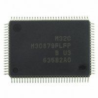
Manufacturer Part Number
M30879FLFP#U3
Description
IC M32C/87 MCU FLASH 100QFP
Manufacturer
Renesas Electronics America
Series
M16C™ M32C/80r
Datasheets
1.M3087BFLGPU3.pdf
(93 pages)
2.M3087BFLGPU3.pdf
(629 pages)
3.M3087BFLGPU3.pdf
(364 pages)
Specifications of M30879FLFP#U3
Core Processor
M32C/80
Core Size
16/32-Bit
Speed
32MHz
Connectivity
CAN, EBI/EMI, I²C, IEBus, IrDA, SIO, UART/USART
Peripherals
DMA, POR, PWM, WDT
Number Of I /o
85
Program Memory Size
1MB (1M x 8)
Program Memory Type
FLASH
Ram Size
48K x 8
Voltage - Supply (vcc/vdd)
3 V ~ 5.5 V
Data Converters
A/D 26x10b; D/A 2x8b
Oscillator Type
Internal
Operating Temperature
-40°C ~ 85°C
Package / Case
100-QFP
For Use With
R0K330879S001BE - KIT DEV RSK M32C/87R0K330879S000BE - KIT DEV RSK M32C/87
Lead Free Status / RoHS Status
Lead free / RoHS Compliant
Eeprom Size
-
Available stocks
Company
Part Number
Manufacturer
Quantity
Price


Rev.
REVISION HISTORY
1.50
Oct 20, 2007
Date
9, 14, 15
19-22
34-39
11,17
Page
2-5
6-7
All
26
45
27
34
41
42
1
2
8
All in this manual
• Descriptions and formats unified
• Notation of numbers changed (e.g. 00
• Notation of pin name changed
• [Term changed]
Overview
• Header SINGLE-CHIP 16/32-BIT CMOS MICROCOMPUTER
• 1.1 Features title added; 1.1 Applications changed to 1.1.1 Applications
• 1.2 Performance Overview changed to 1.1.2 Specifications
• Tables 1.1 to 1.4 Structure, descriptions in Specification field, NOTE, and
• Real-Time Port Item deleted; ROM Correction Function Item added
• 1.3 Block Diagram moved following the 1.2 Product List
• 1.2 Product List Tables revised; NOTE 1 added
• Figures 1.3 to 1.5 Arrows for VSS and VCC deleted; NOTES partially
• Tables 1.9 and 1.13 CLKOUT pin moved from Bus Control Pin column to
• Tables 1.15 to 1.19 Descriptions revised; NOTE 1 added
Memory
• Text partially modified
SFR
• Tables 4.8 to 4.13 NOTE “Set the PM13 bit in the PM1 register to 1 (2 wait
• Table 4.19 The PSL5 register added to the Address field of 03BBh item;
• [Register names changed]
Serial I/O → Serial interface
Clock synchronous serial I/O mode → Clock synchronous mode
Clock asynchronous serial I/O mode → Clock asynchronous mode
Clock synchronous variable length → Variable data length clock
Voltage detection circuit → Power supply voltage detection function
Low voltage detection interrupt → Vdet4 detection interrupt
Brown-out detection reset → Vdet3 detection function
value partially revised or deleted
modified
Control Pin column
(e.g. RTP00 → RTP_0, A15(/D15) → [A15/D15])
synchronous
states for SFR area) before accessing the CAN-associated registers.”
added
the PSL7 register added to the Address field of 03BFh item
002Fh Low Voltage Detection Interrupt Register → Vdet4 Detection
01C1h UART5 Bit Rate Register → UART5 Baud Rate Register
01C9h UART6 Bit Rate Register → UART6 Baud Rate Register
01D0h UART5, UART6 Transmit/Receive Control Register 2 → UART5,
01DBh to 01D8h Pulse Output Data Register → RTP Output Buffer
0303h to 0302h Timer A1-1 Register → Timer A11 Register
0305h to 0304h Timer A2-1 Register → Timer A21 Register
0307h to 0306h Timer A4-1 Register → Timer A41 Register
0340h Count Start Flag → Count Start Register
0341h Clock Prescaler Reset Flag → Clock Prescaler Reset Register
→ RENESAS MCU
Interrupt Register
UART6 Transmit/Receive Control Register
Register
M32C/87 Group Datasheet
A - 3
Description
Summary
2
→ 00b, FF
16
→ FFh)
Related parts for M30879FLFP#U3
Image
Part Number
Description
Manufacturer
Datasheet
Request
R

Part Number:
Description:
KIT STARTER FOR M16C/29
Manufacturer:
Renesas Electronics America
Datasheet:

Part Number:
Description:
KIT STARTER FOR R8C/2D
Manufacturer:
Renesas Electronics America
Datasheet:

Part Number:
Description:
R0K33062P STARTER KIT
Manufacturer:
Renesas Electronics America
Datasheet:

Part Number:
Description:
KIT STARTER FOR R8C/23 E8A
Manufacturer:
Renesas Electronics America
Datasheet:

Part Number:
Description:
KIT STARTER FOR R8C/25
Manufacturer:
Renesas Electronics America
Datasheet:

Part Number:
Description:
KIT STARTER H8S2456 SHARPE DSPLY
Manufacturer:
Renesas Electronics America
Datasheet:

Part Number:
Description:
KIT STARTER FOR R8C38C
Manufacturer:
Renesas Electronics America
Datasheet:

Part Number:
Description:
KIT STARTER FOR R8C35C
Manufacturer:
Renesas Electronics America
Datasheet:

Part Number:
Description:
KIT STARTER FOR R8CL3AC+LCD APPS
Manufacturer:
Renesas Electronics America
Datasheet:
Part Number:
Description:
KIT STARTER FOR RX610
Manufacturer:
Renesas Electronics America
Datasheet:

Part Number:
Description:
KIT STARTER FOR R32C/118
Manufacturer:
Renesas Electronics America
Datasheet:

Part Number:
Description:
KIT DEV RSK-R8C/26-29
Manufacturer:
Renesas Electronics America
Datasheet:

Part Number:
Description:
KIT STARTER FOR SH7124
Manufacturer:
Renesas Electronics America
Datasheet:

Part Number:
Description:
KIT STARTER FOR H8SX/1622
Manufacturer:
Renesas Electronics America
Datasheet:

Part Number:
Description:
KIT DEV FOR SH7203
Manufacturer:
Renesas Electronics America
Datasheet: