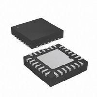
ATTINY48-MMU Atmel, ATTINY48-MMU Datasheet - Page 17

ATTINY48-MMU
Manufacturer Part Number
ATTINY48-MMU
Description
MCU AVR 5K FLASH 12MHZ 28-QFN
Manufacturer
Atmel
Series
AVR® ATtinyr
Specifications of ATTINY48-MMU
Core Processor
AVR
Core Size
8-Bit
Speed
12MHz
Connectivity
I²C, SPI
Peripherals
Brown-out Detect/Reset, POR, WDT
Number Of I /o
24
Program Memory Size
4KB (2K x 16)
Program Memory Type
FLASH
Eeprom Size
64 x 8
Ram Size
256 x 8
Voltage - Supply (vcc/vdd)
1.8 V ~ 5.5 V
Data Converters
A/D 6x10b
Oscillator Type
Internal
Operating Temperature
-40°C ~ 85°C
Package / Case
28-VQFN Exposed Pad, 28-HVQFN, 28-SQFN, 28-DHVQFN
Processor Series
ATTINY4x
Core
AVR8
Data Bus Width
8 bit
Data Ram Size
256 B
Interface Type
2-Wire, I2S, SPI
Maximum Clock Frequency
12 MHz
Number Of Programmable I/os
24
Number Of Timers
2
Maximum Operating Temperature
+ 85 C
Mounting Style
SMD/SMT
3rd Party Development Tools
EWAVR, EWAVR-BL
Development Tools By Supplier
ATAVRDRAGON, ATSTK500, ATSTK600, ATAVRISP2, ATAVRONEKIT
Minimum Operating Temperature
- 40 C
On-chip Adc
10 bit, 6 Channel
Package
28VQFN EP
Device Core
AVR
Family Name
ATtiny
Maximum Speed
12 MHz
Operating Supply Voltage
2.5|3.3|5 V
For Use With
ATAVRDRAGON - KIT DRAGON 32KB FLASH MEM AVR
Lead Free Status / RoHS Status
Lead free / RoHS Compliant
- Current page: 17 of 302
- Download datasheet (9Mb)
5. Memories
5.1
8008G–AVR–04/11
Program Memory (Flash)
The AVR architecture makes a distinction between program memory and data memory, locating
each memory type in a separate address space. Executable code is located in non-volatile pro-
gram memory (Flash), whereas data can be placed in either volatile (SRAM) or non-volatile
memory (EEPROM). See
Figure 5-1.
All memory spaces are linear and regular.
ATtiny48/88 contains 4/8K byte of on-chip, in-system reprogrammable Flash memory for pro-
gram storage. Flash memories are non-volatile, i.e. they retain stored information even when not
powered.
Since all AVR instructions are 16 or 32 bits wide, the Flash is organized as 4096/8192 x 16 bits.
The Program Counter (PC) is 11/12 bits wide, thus capable of addressing all 4096/8192 loca-
tions of program memory, as illustrated in
Table 5-1.
Constant tables can be allocated within the entire address space of program memory. See
instructions LPM (Load Program Memory), and SPM (Store Program Memory) in
Summary” on page
device, as described in
Timing diagrams for instruction fetch and execution are presented in
ing” on page
The Flash memory has a minimum endurance of 10,000 write/erase cycles.
Device
ATtiny48
ATtiny88
PROGRAM MEMORY
FLASH
12.
Memory Overview.
Size of Program Memory (Flash).
281. Flash program memory can also be programmed from an external
“External Programming” on page
Figure
Flash Size
4KB
8KB
5-1, below.
GENERAL PURPOSE
I/O REGISTER FILE
I/O REGISTER FILE
DATA MEMORY
REGISTER FILE
Table
EXTENDED
SRAM
5-1, below.
191.
Address Range
0x0000 – 0x07FF
0x0000 – 0x0FFF
“Instruction Execution Tim-
ATtiny48/88
DATA MEMORY
EEPROM
“Instruction Set
17
Related parts for ATTINY48-MMU
Image
Part Number
Description
Manufacturer
Datasheet
Request
R

Part Number:
Description:
Manufacturer:
Atmel Corporation
Datasheet:

Part Number:
Description:
MCU AVR 4K ISP FLASH 1.8V 32TQFP
Manufacturer:
Atmel
Datasheet:

Part Number:
Description:
MCU AVR 4K ISP FLASH 1.8V 32-QFN
Manufacturer:
Atmel
Datasheet:

Part Number:
Description:
MCU AVR 4K ISP FLASH 1.8V 28-DIP
Manufacturer:
Atmel
Datasheet:

Part Number:
Description:
MCU AVR 4KB FLASH 12MHZ 32TQFP
Manufacturer:
Atmel
Datasheet:

Part Number:
Description:
MCU AVR 4KB FLASH 12MHZ 32QFN
Manufacturer:
Atmel
Datasheet:

Part Number:
Description:
MCU AVR 4KB FLASH 12MHZ 28-VQFN
Manufacturer:
Atmel
Datasheet:

Part Number:
Description:
MCU AVR 4KB FLASH 12MHZ 28QFN
Manufacturer:
Atmel
Datasheet:

Part Number:
Description:
8-bit Microcontrollers - MCU 4KB FL,64B EE, 256B SRAM-12MHz
Manufacturer:
Atmel

Part Number:
Description:
8-bit Microcontrollers - MCU Microcontroller
Manufacturer:
Atmel

Part Number:
Description:
Manufacturer:
Atmel Corporation
Datasheet:


