PIC24F04KA201T-I/MQ Microchip Technology, PIC24F04KA201T-I/MQ Datasheet - Page 11
PIC24F04KA201T-I/MQ
Manufacturer Part Number
PIC24F04KA201T-I/MQ
Description
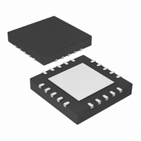
IC PIC MCU FLASH 512KX4 20-QFN
Manufacturer
Microchip Technology
Series
PIC® XLP™ 24Fr
Datasheets
1.PIC24F04KA201-ISS.pdf
(8 pages)
2.PIC24F04KA201-ISS.pdf
(48 pages)
3.PIC24F04KA201-ISS.pdf
(224 pages)
4.PIC24F04KA201-ISS.pdf
(26 pages)
Specifications of PIC24F04KA201T-I/MQ
Program Memory Type
FLASH
Program Memory Size
4KB (1.375K x 24)
Package / Case
20-QFN
Core Processor
PIC
Core Size
16-Bit
Speed
32MHz
Connectivity
I²C, IrDA, SPI, UART/USART
Peripherals
Brown-out Detect/Reset, HLVD, POR, PWM, WDT
Number Of I /o
18
Ram Size
512 x 8
Voltage - Supply (vcc/vdd)
1.8 V ~ 3.6 V
Data Converters
A/D 9x10b
Oscillator Type
Internal
Operating Temperature
-40°C ~ 85°C
Processor Series
PIC24F
Core
PIC
Data Bus Width
16 bit
Data Ram Size
512 B
Interface Type
I2C/SPI/UART
Maximum Clock Frequency
32 MHz
Number Of Programmable I/os
18
Number Of Timers
3
Operating Supply Voltage
1.8 V to 3.6 V
Maximum Operating Temperature
+ 85 C
Mounting Style
SMD/SMT
3rd Party Development Tools
52713-733, 52714-737, 53276-922, EWDSPIC
Development Tools By Supplier
PG164130, DV164035, DV244005, DV164005, DM240001
Minimum Operating Temperature
- 40 C
On-chip Adc
9-ch x 10-bit
Lead Free Status / RoHS Status
Lead free / RoHS Compliant
Eeprom Size
-
Lead Free Status / Rohs Status
Lead free / RoHS Compliant


TABLE 3-5:
2010 Microchip Technology Inc.
Step 4: Load W0:W5 with the next 4 instruction words to program.
Step 5: Set the Read Pointer (W6) and load the (next set of) write latches.
Step 6: Repeat Steps 3 though 5, eight times, to load the write latches for 32 instructions.
Step 7: Initiate the write cycle.
Step 8: Repeat this step to poll the WR bit (bit 15 of NVMCON) until it is cleared by the hardware.
Step 9: Reset device internal PC.
Step 10: Repeat Steps 3 through 9 until the entire code memory is programmed.
Command
(Binary)
0000
0000
0000
0000
0000
0000
0000
0000
0000
0000
0000
0000
0000
0000
0000
0000
0000
0000
0000
0000
0000
0000
0000
0000
0000
0000
0000
0000
0000
0000
0000
0000
0000
0000
0000
0000
0000
0000
0000
0000
0001
0000
0000
0000
SERIAL INSTRUCTION EXECUTION FOR WRITING CODE MEMORY (CONTINUED)
2xxxx0
2xxxx1
2xxxx2
2xxxx3
2xxxx4
2xxxx5
EB0300
000000
BB0BB6
000000
000000
BBDBB6
000000
000000
BBEBB6
000000
000000
BB1BB6
000000
000000
BB0BB6
000000
000000
BBDBB6
000000
000000
BBEBB6
000000
000000
BB1BB6
000000
000000
A8E761
000000
000000
040200
000000
803B02
883C22
000000
<VISI>
000000
040200
000000
(Hex)
Data
MOV
MOV
MOV
MOV
MOV
MOV
CLR
NOP
TBLWTL
NOP
NOP
TBLWTH.B
NOP
NOP
TBLWTH.B
NOP
NOP
TBLWTL
NOP
NOP
TBLWTL
NOP
NOP
TBLWTH.B
NOP
NOP
TBLWTH.B
NOP
NOP
TBLWTL
NOP
NOP
BSET
NOP
NOP
GOTO
NOP
MOV
MOV
NOP
Clock out contents of the VISI register.
NOP
GOTO
NOP
#<LSW0>, W0
#<MSB1:MSB0>, W1
#<LSW1>, W2
#<LSW2>, W3
#<MSB3:MSB2>, W4
#<LSW3>, W5
W6
[W6++], [W7]
[W6++], [W7++]
[W6++], [++W7]
[W6++], [W7++]
[W6++], [W7]
[W6++], [W7++]
[W6++], [++W7]
[W6++], [W7++]
NVMCON, #WR
0x200
NVMCON, W2
W2, VISI
0x200
Description
PIC24FXXKA2XX
DS39991A-page 11
Related parts for PIC24F04KA201T-I/MQ
Image
Part Number
Description
Manufacturer
Datasheet
Request
R

Part Number:
Description:
Manufacturer:
Microchip Technology Inc.
Datasheet:
Part Number:
Description:
Manufacturer:
Microchip Technology Inc.
Datasheet:
Part Number:
Description:
Manufacturer:
Microchip Technology Inc.
Datasheet:
Part Number:
Description:
Manufacturer:
Microchip Technology Inc.
Datasheet:
Part Number:
Description:
Manufacturer:
Microchip Technology Inc.
Datasheet:
Part Number:
Description:
Manufacturer:
Microchip Technology Inc.
Datasheet:
Part Number:
Description:
Manufacturer:
Microchip Technology Inc.
Datasheet:
Part Number:
Description:
Manufacturer:
Microchip Technology Inc.
Datasheet: