PIC16LF1826-I/MV Microchip Technology, PIC16LF1826-I/MV Datasheet - Page 248
PIC16LF1826-I/MV
Manufacturer Part Number
PIC16LF1826-I/MV
Description
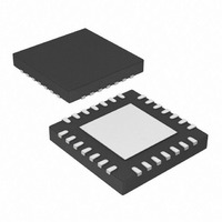
IC MCU 8BIT FLASH 28UQFN
Manufacturer
Microchip Technology
Series
PIC® XLP™ 16Fr
Datasheet
1.PIC16F1826-IP.pdf
(406 pages)
Specifications of PIC16LF1826-I/MV
Core Size
8-Bit
Program Memory Size
3.5KB (2K x 14)
Core Processor
PIC
Speed
32MHz
Connectivity
I²C, SPI, UART/USART
Peripherals
Brown-out Detect/Reset, POR, PWM, WDT
Number Of I /o
16
Program Memory Type
FLASH
Eeprom Size
256 x 8
Ram Size
256 x 8
Voltage - Supply (vcc/vdd)
1.8 V ~ 3.6 V
Data Converters
A/D 12x10b
Oscillator Type
Internal
Operating Temperature
-40°C ~ 85°C
Package / Case
28-UFQFN Exposed Pad
Controller Family/series
PIC16LF
No. Of I/o's
16
Eeprom Memory Size
256Byte
Ram Memory Size
256Byte
Cpu Speed
32MHz
No. Of Timers
3
Processor Series
PIC16LF
Core
PIC
Data Ram Size
256 B
Maximum Clock Frequency
32 KHz
Number Of Programmable I/os
16
Number Of Timers
3
Operating Supply Voltage
1.8 V to 3.6 V
Maximum Operating Temperature
+ 125 C
3rd Party Development Tools
52715-96, 52716-328, 52717-734
Development Tools By Supplier
PG164130, DV164035, DV244005, DV164005
Minimum Operating Temperature
- 40 C
On-chip Adc
10 bit, 12 Channel
On-chip Dac
5 bit
Lead Free Status / RoHS Status
Lead free / RoHS Compliant
Lead Free Status / RoHS Status
Lead free / RoHS Compliant


PIC16F/LF1826/27
24.4.9
The 9th SCLx pulse for any transferred byte in I
dedicated as an Acknowledge. It allows receiving
devices to respond back to the transmitter by pulling
the SDAx line low. The transmitter must release con-
trol of the line during this time to shift in the response.
The Acknowledge (ACK) is an active-low signal, pull-
ing the SDAx line low indicated to the transmitter that
the device has received the transmitted data and is
ready to receive more.
The result of an ACK is placed in the ACKSTAT bit of
the SSPxCON2 register.
Slave software, when the AHEN and DHEN bits are
set, allow the user to set the ACK value sent back to
the transmitter. The ACKDT bit of the SSPxCON2 reg-
ister is set/cleared to determine the response.
Slave hardware will generate an ACK response if the
AHEN and DHEN bits of the SSPxCON3 register are
clear.
There are certain conditions where an ACK will not be
sent by the slave. If the BF bit of the SSPxSTAT regis-
ter or the SSPxOV bit of the SSPxCON1 register are
set when a byte is received.
When the module is addressed, after the 8th falling
edge of SCLx on the bus, the ACKTIM bit of the
SSPxCON3 register is set. The ACKTIM bit indicates
the acknowledge time of the active bus. The ACKTIM
Status bit is only active when the AHEN bit or DHEN
bit is enabled.
DS41391C-page 248
ACKNOWLEDGE SEQUENCE
2
C is
Preliminary
24.5
The MSSPx Slave mode operates in one of four
modes selected in the SSPxM bits of SSPxCON1 reg-
ister. The modes can be divided into 7-bit and 10-bit
Addressing mode. 10-bit Addressing modes operate
the same as 7-bit with some additional overhead for
handling the larger addresses.
Modes with Start and Stop bit interrupts operated the
same as the other modes with SSPxIF additionally
getting set upon detection of a Start, Restart, or Stop
condition.
24.5.1
The SSPxADD register (Register 24-6) contains the
Slave mode address. The first byte received after a
Start or Restart condition is compared against the
value stored in this register. If the byte matches, the
value is loaded into the SSPxBUF register and an
interrupt is generated. If the value does not match, the
module goes idle and no indication is given to the soft-
ware that anything happened.
The SSPx Mask register (Register 24-5) affects the
address matching process.
“SSPx Mask Register” for more information.
24.5.1.1
In 7-bit Addressing mode, the LSb of the received data
byte is ignored when determining if there is an address
match.
24.5.1.2
In 10-bit Addressing mode, the first received byte is
compared to the binary value of ‘1 1 1 1 0 A9 A8 0’. A9
and A8 are the two MSb of the 10-bit address and
stored in bits 2 and 1 of the SSPxADD register.
After the acknowledge of the high byte the UA bit is set
and SCLx is held low until the user updates SSPxADD
with the low address. The low address byte is clocked
in and all 8 bits are compared to the low address value
in SSPxADD. Even if there is not an address match;
SSPxIF and UA are set, and SCLx is held low until
SSPxADD is updated to receive a high byte again.
When SSPxADD is updated the UA bit is cleared. This
ensures the module is ready to receive the high
address byte on the next communication.
A high and low address match as a write request is
required at the start of all 10-bit addressing communi-
cation. A transmission can be initiated by issuing a
Restart once the slave is addressed, and clocking in
the high address with the R/W bit set. The slave hard-
ware will then acknowledge the read request and pre-
pare to clock out data. This is only valid for a slave
after it has received a complete high and low address
byte match.
I
SLAVE MODE ADDRESSES
2
C
I
I
2
2
C Slave 7-bit Addressing Mode
C Slave 10-bit Addressing Mode
SLAVE MODE OPERATION
2010 Microchip Technology Inc.
See
Section 24.5.9
Related parts for PIC16LF1826-I/MV
Image
Part Number
Description
Manufacturer
Datasheet
Request
R

Part Number:
Description:
IC, 8BIT MCU, PIC16LF, 32MHZ, QFN-28
Manufacturer:
Microchip Technology
Datasheet:

Part Number:
Description:
IC, 8BIT MCU, PIC16LF, 32MHZ, QFN-28
Manufacturer:
Microchip Technology
Datasheet:

Part Number:
Description:
IC, 8BIT MCU, PIC16LF, 32MHZ, DIP-18
Manufacturer:
Microchip Technology
Datasheet:

Part Number:
Description:
IC, 8BIT MCU, PIC16LF, 20MHZ, TQFP-44
Manufacturer:
Microchip Technology
Datasheet:
Part Number:
Description:
7 KB Flash, 384 Bytes RAM, 32 MHz Int. Osc, 16 I/0, Enhanced Mid Range Core, Nan
Manufacturer:
Microchip Technology

Part Number:
Description:
14KB Flash, 512B RAM, LCD, 11x10b ADC, EUSART, NanoWatt XLP 28 SOIC .300in T/R
Manufacturer:
Microchip Technology
Datasheet:
Part Number:
Description:
14KB Flash, 512B RAM, LCD, 11x10b ADC, EUSART, NanoWatt XLP 28 SSOP .209in T/R
Manufacturer:
Microchip Technology
Datasheet:
Part Number:
Description:
MCU PIC 14KB FLASH XLP 28-SSOP
Manufacturer:
Microchip Technology
Part Number:
Description:
MCU PIC 14KB FLASH XLP 28-SOIC
Manufacturer:
Microchip Technology
Part Number:
Description:
MCU PIC 512B FLASH XLP 28-UQFN
Manufacturer:
Microchip Technology
Part Number:
Description:
MCU PIC 14KB FLASH XLP 28-SPDIP
Manufacturer:
Microchip Technology

Part Number:
Description:
MCU 7KB FLASH 256B RAM 40-UQFN
Manufacturer:
Microchip Technology
Part Number:
Description:
MCU 7KB FLASH 256B RAM 44-TQFP
Manufacturer:
Microchip Technology

Part Number:
Description:
MCU 14KB FLASH 1KB RAM 28-UQFN
Manufacturer:
Microchip Technology
Part Number:
Description:
MCU PIC 14KB FLASH XLP 40-UQFN
Manufacturer:
Microchip Technology