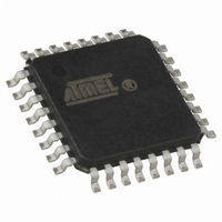
AT89LP828-20AU Atmel, AT89LP828-20AU Datasheet - Page 69

AT89LP828-20AU
Manufacturer Part Number
AT89LP828-20AU
Description
MCU 8051 8K FLASH SPI 32TQFP
Manufacturer
Atmel
Series
89LPr
Datasheet
1.AT89LP428-20AU.pdf
(149 pages)
Specifications of AT89LP828-20AU
Core Processor
8051
Core Size
8-Bit
Speed
20MHz
Connectivity
SPI, UART/USART
Peripherals
Brown-out Detect/Reset, POR, PWM, WDT
Number Of I /o
30
Program Memory Size
8KB (8K x 8)
Program Memory Type
FLASH
Eeprom Size
1K x 8
Ram Size
768 x 8
Voltage - Supply (vcc/vdd)
2.4 V ~ 5.5 V
Oscillator Type
Internal
Operating Temperature
-40°C ~ 85°C
Package / Case
32-TQFP, 32-VQFP
Processor Series
AT89x
Core
8051
Data Bus Width
8 bit
Data Ram Size
768 B
Interface Type
2-Wire, SPI
Maximum Clock Frequency
20 MHz
Number Of Programmable I/os
30
Number Of Timers
3
Maximum Operating Temperature
+ 85 C
Mounting Style
SMD/SMT
3rd Party Development Tools
PK51, CA51, A51, ULINK2
Development Tools By Supplier
AT89ISP
Minimum Operating Temperature
- 40 C
Lead Free Status / RoHS Status
Lead free / RoHS Compliant
Data Converters
-
Lead Free Status / Rohs Status
Details
Available stocks
Company
Part Number
Manufacturer
Quantity
Price
Company:
Part Number:
AT89LP828-20AU
Manufacturer:
Atmel
Quantity:
360
13.4.1
3654A–MICRO–8/09
Asymmetrical PWM
and precision is made by changing the TOP value of the timer. The CCA PWM always uses the
greatest precision allowable for the selected output frequency, as compared to Timer 0 and 1
whose PWMs are fixed at 8-bit precision regardless of frequency.
Figure 13-7. CCA PWM Mode Diagram
For Asymmetrical PWM, Timer 2 should be configured for Auto-reload mode and Count Mode 1
(CP/RL2 = 0, DCEN = 0, T2CM1-0 = 01B). Asymmetrical PWM uses single slope operation as
shown in
TOM. In non-inverting mode, the output CCx is set on the compare match between Timer 2
(TL2, TH2) and the channel data register (CCxL, CCxH), and cleared at BOTTOM. In inverting
mode, the output CCx is cleared on the compare match between Timer 2 and the data register,
and set at BOTTOM. The resulting asymmetrical output waveform is left-edge aligned.
The TOP value in RCAP2L and RCAP2H is double buffered such that the output frequency is
only updated at the TOP to BOTTOM overflow. The channel data register (CCxL, CCxH) is also
double-buffered such that the duty cycle is only updated at the TOP to BOTTOM overflow to pre-
vent glitches. The output frequency and duty cycle for asymmetrical PWM are given by the
following equations:
The extreme compare values represent special cases when generating a PWM waveform. If the
compare value is set equal to (or greater than) TOP, the output will remain low or high for non-
inverting and inverting modes, respectively. If the compare value is set to BOTTOM (0000H), the
output will remain high or low for non-inverting and inverting modes, respectively.
Figure
Non-Inverting:
T2CCL
CCxL
Shadow
TL2
13-8. The timer counts up from BOTTOM to TOP and then restarts from BOT-
Inverting:
Shadow
T2CCH
CCxH
Shadow
TH2
Duty Cycle
f
OUT
=
Duty Cycle
=
--------------------------------------------------------------- -
{
RCAP2H RCAP2L
Oscillator Frequency
=
T2CCC
CCCx
100%
=
,
100%
×
{
------------------------------------------------------------------------------------------------------------ -
RCAP2H RCAP2L
×
}
--------------------------------------------------------------- -
{
CCFx
+
RCAP2H RCAP2L
{
1
RCAP2H RCAP2L
CIENx
,
×
{
CxM
CCxH CCxL
-------------------- -
TPS
2-0
,
1
+
,
,
}
1
AT89LP428/828
–
{
}
CCxH CCxL
}
+
}
1
+
,
1
Interrupt
CCx (P2.x)
}
+
1
69


