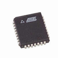
AT89LP828-20JU Atmel, AT89LP828-20JU Datasheet - Page 42

AT89LP828-20JU
Manufacturer Part Number
AT89LP828-20JU
Description
MCU 8051 8K FLASH SPI 32PLCC
Manufacturer
Atmel
Series
89LPr
Datasheet
1.AT89LP428-20AU.pdf
(149 pages)
Specifications of AT89LP828-20JU
Core Processor
8051
Core Size
8-Bit
Speed
20MHz
Connectivity
SPI, UART/USART
Peripherals
Brown-out Detect/Reset, POR, PWM, WDT
Number Of I /o
30
Program Memory Size
8KB (8K x 8)
Program Memory Type
FLASH
Eeprom Size
1K x 8
Ram Size
768 x 8
Voltage - Supply (vcc/vdd)
2.4 V ~ 5.5 V
Oscillator Type
Internal
Operating Temperature
-40°C ~ 85°C
Package / Case
32-PLCC
Processor Series
AT89x
Core
8051
Data Bus Width
8 bit
Data Ram Size
768 B
Interface Type
2-Wire, SPI
Maximum Clock Frequency
20 MHz
Number Of Programmable I/os
30
Number Of Timers
3
Maximum Operating Temperature
+ 85 C
Mounting Style
SMD/SMT
3rd Party Development Tools
PK51, CA51, A51, ULINK2
Development Tools By Supplier
AT89ISP
Minimum Operating Temperature
- 40 C
Lead Free Status / RoHS Status
Lead free / RoHS Compliant
Data Converters
-
Lead Free Status / Rohs Status
Details
Available stocks
Company
Part Number
Manufacturer
Quantity
Price
11.1
11.2
42
Mode 0 – Variable Width Timer/Counter
Mode 1 – 16-bit Auto-Reload Timer/Counter
AT89LP428/828
Both Timers in Mode 0 are 8-bit Counters with a variable prescaler. The prescaler may vary from
1 to 8 bits depending on the PSC bits in TCONB, giving the timer a range of 9 to 16 bits.
By default the timer is configured as a 13-bit timer compatible to Mode 0 in the standard 8051.
Figure 11-1
rolls over from all “1”s to all “0”s, it sets the Timer interrupt flag TF1. The counter input is enabled
to the Timer when TR1 = 1 and either GATE = 0 or INT1 = 1. Setting GATE = 1 allows the Timer
to be controlled by external input INT1, to facilitate pulse width measurements. TR1 is a control
bit in the Special Function Register TCON. GATE is in TMOD. The 13-bit register consists of all
8 bits of TH1 and the lower 5 bits of TL1. The upper 3 bits of TL1 are indeterminate and should
be ignored. Setting the run flag (TR1) does not clear the registers.
Note:
Figure 11-1. Timer/Counter 1 Mode 0: Variable Width Counter
Mode 0 operation is the same for Timer 0 as for Timer 1, except that TR0, TF0 and INT0 replace
the corresponding Timer 1 signals in
Timer 1 (TMOD.7) and one for Timer 0 (TMOD.3).
In Mode 1 the Timers are configured for 16-bit auto-reload. The Timer register is run with all
16 bits. The 16-bit reload value is stored in the high and low reload registers (RH1/RL1). The
clock is applied to the combined high and low timer registers (TH1/TL1). As clock pulses are
received, the timer counts up: 0000H, 0001H, 0002H, etc. An overflow occurs on the FFFFH-to-
0000H transition, upon which the timer register is reloaded with the value from RH1/RL1 and the
overflow flag bit in TCON is set. See
gives the full 16-bit timer period compatible with the standard 8051. Mode 1 operation is the
same for Timer/Counter 0.
INT1 Pin
T1 Pin
RH1/RL1 are not required by Timer 1 during Mode 0 and may be used as temporary storage
registers.
GATE
OSC
shows the Mode 0 operation as it applies to Timer 1 in 13-bit mode. As the count
Mode 0:
Mode 1:
TR1
÷TPS
Time-out Period
C/T = 0
C/T = 1
Time-out Period
Control
Figure
Figure
=
11-2. The reload registers default to 0000H, which
=
11-1. There are two different GATE bits, one for
------------------------------------------------------ -
Oscillator Frequency
(
---------------------------------------------------------
Oscillator Frequency
65536
256
(8 Bits)
TL1
×
–
2
{
PSC0
RH0 RL0
(8 Bits)
,
+
TH1
1
PSC1
}
×
)
×
(
TPS
(
TPS
TF1
+
1
+
)
1
3654A–MICRO–8/09
)
Interrupt


