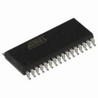
AT90PWM316-16SU Atmel, AT90PWM316-16SU Datasheet - Page 91

AT90PWM316-16SU
Manufacturer Part Number
AT90PWM316-16SU
Description
MCU AVR 16K ISP FLSH 16MHZ32SOIC
Manufacturer
Atmel
Series
AVR® 90PWM Lightingr
Datasheet
1.AT90PWM216-16SU.pdf
(359 pages)
Specifications of AT90PWM316-16SU
Core Processor
AVR
Core Size
8-Bit
Speed
16MHz
Connectivity
SPI, UART/USART
Peripherals
Brown-out Detect/Reset, POR, PWM, WDT
Number Of I /o
27
Program Memory Size
16KB (16K x 8)
Program Memory Type
FLASH
Eeprom Size
512 x 8
Ram Size
1K x 8
Voltage - Supply (vcc/vdd)
2.7 V ~ 5.5 V
Data Converters
A/D 11x10b; D/A 1x10b
Oscillator Type
Internal
Operating Temperature
-40°C ~ 105°C
Package / Case
32-SOIC (7.5mm Width)
Processor Series
AT90PWMx
Core
AVR8
Data Bus Width
8 bit
Data Ram Size
1 KB
Interface Type
SPI, UART
Maximum Clock Frequency
16 MHz
Number Of Programmable I/os
53
Number Of Timers
2
Operating Supply Voltage
2.7 V to 5.5 V
Maximum Operating Temperature
+ 105 C
Mounting Style
SMD/SMT
3rd Party Development Tools
EWAVR, EWAVR-BL
Development Tools By Supplier
ATAVRDRAGON, ATSTK500, ATSTK600, ATAVRISP2, ATAVRONEKIT, ATAVRFBKIT, ATAVRISP2
Minimum Operating Temperature
- 40 C
On-chip Adc
10 bit, 11 Channel
Package
32SOIC
Device Core
AVR
Family Name
90P
Maximum Speed
16 MHz
For Use With
ATSTK600-SOIC - STK600 SOCKET/ADAPTER FOR SOIC770-1007 - ISP 4PORT ATMEL AVR MCU SPI/JTAG770-1005 - ISP 4PORT FOR ATMEL AVR MCU JTAG770-1004 - ISP 4PORT FOR ATMEL AVR MCU SPIATAVRMC200 - KIT EVAL FOR AT90PWM3 ASYNCATAVRFBKIT - KIT DEMO BALLAST FOR AT90PWM2ATAVRISP2 - PROGRAMMER AVR IN SYSTEM
Lead Free Status / RoHS Status
Lead free / RoHS Compliant
Available stocks
Company
Part Number
Manufacturer
Quantity
Price
Part Number:
AT90PWM316-16SU
Manufacturer:
ATMEL/爱特梅尔
Quantity:
20 000
- Current page: 91 of 359
- Download datasheet (6Mb)
14.6
14.6.1
14.6.2
7710E–AVR–08/10
Modes of Operation
Normal Mode
Clear Timer on Compare Match (CTC) Mode
non-PWM modes refer to
page
A change of the COM0x1:0 bits state will have effect at the first compare match after the bits are
written. For non-PWM modes, the action can be forced to have immediate effect by using the
FOC0x strobe bits.
The mode of operation, i.e., the behavior of the Timer/Counter and the Output Compare pins, is
defined by the combination of the Waveform Generation mode (WGM02:0) and Compare Output
mode (COM0x1:0) bits. The Compare Output mode bits do not affect the counting sequence,
while the Waveform Generation mode bits do. The COM0x1:0 bits control whether the PWM out-
put generated should be inverted or not (inverted or non-inverted PWM). For non-PWM modes
the COM0x1:0 bits control whether the output should be set, cleared, or toggled at a compare
match
For detailed timing information refer to
The simplest mode of operation is the Normal mode (WGM02:0 = 0). In this mode the counting
direction is always up (incrementing), and no counter clear is performed. The counter simply
overruns when it passes its maximum 8-bit value (TOP = 0xFF) and then restarts from the bot-
tom (0x00). In normal operation the Timer/Counter Overflow Flag (TOV0) will be set in the same
timer clock cycle as the TCNT0 becomes zero. The TOV0 Flag in this case behaves like a ninth
bit, except that it is only set, not cleared. However, combined with the timer overflow interrupt
that automatically clears the TOV0 Flag, the timer resolution can be increased by software.
There are no special cases to consider in the Normal mode, a new counter value can be written
anytime.
The Output Compare unit can be used to generate interrupts at some given time. Using the Out-
put Compare to generate waveforms in Normal mode is not recommended, since this will
occupy too much of the CPU time.
In Clear Timer on Compare or CTC mode (WGM02:0 = 2), the OCR0A Register is used to
manipulate the counter resolution. In CTC mode the counter is cleared to zero when the counter
value (TCNT0) matches the OCR0A. The OCR0A defines the top value for the counter, hence
also its resolution. This mode allows greater control of the compare match output frequency. It
also simplifies the operation of counting external events.
The timing diagram for the CTC mode is shown in
increases until a compare match occurs between TCNT0 and OCR0A, and then counter
(TCNT0) is cleared.
97, and for phase correct PWM refer to
(See “Compare Match Output Unit” on page
Table 14-2 on page
“Timer/Counter Timing Diagrams” on page
Table 14-4 on page
97. For fast PWM mode, refer to
90.).
Figure
14-5. The counter value (TCNT0)
AT90PWM216/316
98.
Table 14-3 on
95.
91
Related parts for AT90PWM316-16SU
Image
Part Number
Description
Manufacturer
Datasheet
Request
R

Part Number:
Description:
IC AVR MCU FLASH 8K 32QFN
Manufacturer:
Atmel
Datasheet:

Part Number:
Description:
IC AVR MCU FLASH 8K 32SOIC
Manufacturer:
Atmel
Datasheet:

Part Number:
Description:
MCU AVR 8K FLASH 16MHZ 32-QFN
Manufacturer:
Atmel
Datasheet:

Part Number:
Description:
DEV KIT FOR AVR/AVR32
Manufacturer:
Atmel
Datasheet:

Part Number:
Description:
INTERVAL AND WIPE/WASH WIPER CONTROL IC WITH DELAY
Manufacturer:
ATMEL Corporation
Datasheet:

Part Number:
Description:
Low-Voltage Voice-Switched IC for Hands-Free Operation
Manufacturer:
ATMEL Corporation
Datasheet:

Part Number:
Description:
MONOLITHIC INTEGRATED FEATUREPHONE CIRCUIT
Manufacturer:
ATMEL Corporation
Datasheet:

Part Number:
Description:
AM-FM Receiver IC U4255BM-M
Manufacturer:
ATMEL Corporation
Datasheet:

Part Number:
Description:
Monolithic Integrated Feature Phone Circuit
Manufacturer:
ATMEL Corporation
Datasheet:

Part Number:
Description:
Multistandard Video-IF and Quasi Parallel Sound Processing
Manufacturer:
ATMEL Corporation
Datasheet:

Part Number:
Description:
High-performance EE PLD
Manufacturer:
ATMEL Corporation
Datasheet:

Part Number:
Description:
8-bit Flash Microcontroller
Manufacturer:
ATMEL Corporation
Datasheet:


