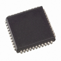
AT89S8253-24JU Atmel, AT89S8253-24JU Datasheet - Page 4

AT89S8253-24JU
Manufacturer Part Number
AT89S8253-24JU
Description
IC MCU 12K FLASH 24MHZ 44-PLCC
Manufacturer
Atmel
Series
89Sr
Datasheet
1.AT89S8253-24PU.pdf
(60 pages)
Specifications of AT89S8253-24JU
Core Processor
8051
Core Size
8-Bit
Speed
24MHz
Connectivity
SPI, UART/USART
Peripherals
POR, WDT
Number Of I /o
32
Program Memory Size
12KB (12K x 8)
Program Memory Type
FLASH
Eeprom Size
2K x 8
Ram Size
256 x 8
Voltage - Supply (vcc/vdd)
2.7 V ~ 5.5 V
Oscillator Type
Internal
Operating Temperature
-40°C ~ 85°C
Package / Case
44-PLCC
Processor Series
AT89x
Core
8051
Data Bus Width
8 bit
Data Ram Size
256 B
Interface Type
SPI/UART
Maximum Clock Frequency
24 MHz
Number Of Programmable I/os
32
Number Of Timers
3
Operating Supply Voltage
2.7 V to 5.5 V
Maximum Operating Temperature
+ 85 C
Mounting Style
SMD/SMT
3rd Party Development Tools
PK51, CA51, A51, ULINK2
Development Tools By Supplier
AT89ISP
Minimum Operating Temperature
- 40 C
Lead Free Status / RoHS Status
Lead free / RoHS Compliant
Data Converters
-
Lead Free Status / Rohs Status
Lead free / RoHS Compliant
Available stocks
Company
Part Number
Manufacturer
Quantity
Price
Company:
Part Number:
AT89S8253-24JU
Manufacturer:
LITTLEFUSE
Quantity:
4 500
Company:
Part Number:
AT89S8253-24JU
Manufacturer:
ATMEL
Quantity:
6
Company:
Part Number:
AT89S8253-24JU
Manufacturer:
ATMEL
Quantity:
5 530
Company:
Part Number:
AT89S8253-24JU
Manufacturer:
ATM
Quantity:
3 290
Company:
Part Number:
AT89S8253-24JU
Manufacturer:
ATMEL
Quantity:
44 616
Part Number:
AT89S8253-24JU
Manufacturer:
ATMEL/爱特梅尔
Quantity:
20 000
3.5
3.6
3.7
3.8
4
PWRGND
Port 0
Port 1
Port 2
AT89S8253
Ground for the 42-PDIP which connects only the I/O Pad Drivers. PWRGND and GND are
weakly connected through the common silicon substrate, but not through any metal links. The
application board must connect both GND and PWRGND to the board ground.
Port 0 is an 8-bit open drain bi-directional I/O port. As an output port, each pin can sink six TTL
inputs. When 1s are written to port 0 pins, the pins can be used as high-impedance inputs.
Port 0 can also be configured to be the multiplexed low-order address/data bus during accesses
to external program and data memory. In this mode, P0 has internal pull-ups.
Port 0 also receives the code bytes during Flash programming and outputs the code bytes dur-
ing program verification. External pull-ups are required during program verification.
Port 1 is an 8-bit bi-directional I/O port with internal pull-ups. The Port 1 output buffers can
sink/source six TTL inputs. When 1s are written to Port 1 pins, they are pulled high by the weak
internal pull-ups and can be used as inputs. As inputs, Port 1 pins that are externally being
pulled low will source current (I
Some Port 1 pins provide additional functions. P1.0 and P1.1 can be configured to be the
timer/counter 2 external count input (P1.0/T2) and the timer/counter 2 trigger input (P1.1/T2EX),
respectively. Furthermore, P1.4, P1.5, P1.6, and P1.7 can be configured as the SPI slave port
select, data input/output and shift clock input/output pins as shown in the following table.
Port 1 also receives the low-order address bytes during Flash programming and verification.
Port 2 is an 8-bit bi-directional I/O port with internal pull-ups. The Port 2 output buffers can
sink/source six TTL inputs. When 1s are written to Port 2 pins, they are pulled high by the weak
internal pull-ups and can be used as inputs. As inputs, Port 2 pins that are externally being
pulled low will source current (I
Port 2 emits the high-order address byte during fetches from external program memory and dur-
ing accesses to external data memory that use 16-bit addresses (MOVX @ DPTR). In this
application, Port 2 uses strong internal pull-ups when emitting 1s. During accesses to external
data memory that use 8-bit addresses (MOVX @ RI), Port 2 emits the contents of the P2
Special Function Register.
Port 2 also receives the high-order address bits and some control signals during Flash
programming and verification.
Port Pin
P1.0
P1.1
P1.4
P1.5
P1.6
P1.7
Alternate Functions
T2 (external count input to Timer/Counter 2), clock-out
T2EX (Timer/Counter 2 capture/reload trigger and direction control)
SS (Slave port select input)
MOSI (Master data output, slave data input pin for SPI channel)
MISO (Master data input, slave data output pin for SPI channel)
SCK (Master clock output, slave clock input pin for SPI channel)
IL
IL
,150
,150
µ
µ
A typical) because of the weak internal pull-ups.
A typical) because of the weak internal pull-ups.
3286P–MICRO–3/10


