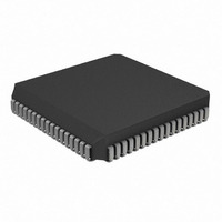
PIC16C924-04I/L Microchip Technology, PIC16C924-04I/L Datasheet - Page 2

PIC16C924-04I/L
Manufacturer Part Number
PIC16C924-04I/L
Description
IC MCU OTP 4KX14 LCD DVR 68PLCC
Manufacturer
Microchip Technology
Series
PIC® 16Cr
Datasheets
1.PIC16F616T-ISL.pdf
(8 pages)
2.PIC16F818-ISO.pdf
(6 pages)
3.PIC16C923-04L.pdf
(189 pages)
4.PIC16LC924-04L.pdf
(10 pages)
Specifications of PIC16C924-04I/L
Core Processor
PIC
Core Size
8-Bit
Speed
4MHz
Connectivity
I²C, SPI
Peripherals
LCD, POR, PWM, WDT
Number Of I /o
25
Program Memory Size
7KB (4K x 14)
Program Memory Type
OTP
Ram Size
176 x 8
Voltage - Supply (vcc/vdd)
4 V ~ 6 V
Data Converters
A/D 5x8b
Oscillator Type
External
Operating Temperature
-40°C ~ 85°C
Package / Case
68-PLCC
Processor Series
PIC16C
Core
PIC
Data Bus Width
8 bit
Data Ram Size
176 B
Interface Type
I2C, SPI
Maximum Clock Frequency
8 MHz
Number Of Programmable I/os
25
Number Of Timers
3
Operating Supply Voltage
2.5 V to 6 V
Maximum Operating Temperature
+ 85 C
Mounting Style
SMD/SMT
3rd Party Development Tools
52715-96, 52716-328, 52717-734
Development Tools By Supplier
ICE2000
Minimum Operating Temperature
- 40 C
On-chip Adc
8 bit, 5 Channel
For Use With
AC164308 - MODULE SKT FOR PM3 68PLCCDVA16XL680 - ADAPTER DEVICE FOR MPLAB-ICEAC164024 - ADAPTER PICSTART PLUS 68PLCCAC164022 - MODULE SKT PROMATEII 68PLCC
Lead Free Status / RoHS Status
Lead free / RoHS Compliant
Eeprom Size
-
Lead Free Status / Rohs Status
Details
Other names
Q701521
Available stocks
Company
Part Number
Manufacturer
Quantity
Price
Company:
Part Number:
PIC16C924-04I/L
Manufacturer:
Microchip Technology
Quantity:
10 000
PIC16C924
4. Module: SSP Module (I
5. Module: SSP (SPI™ Mode)
EXAMPLE 1:
DS80111B-page 2
WAIT
If the bus is active when the I
and the next 8 bits of data on the bus match the
address of the device, then the SSP module will
generate an Acknowledge pulse.
Work around
Before enabling the I
is not active.
The Synchronous Serial Port module in SPI Mas-
ter mode only, allows the transmission of 1 byte of
data at a time. The module must be disabled and
then re-enabled between each byte transmission.
Work around
Once the SSP module has been configured in SPI
Master mode and one byte of data has been trans-
mitted, wait for the interrupt flag bit SSPIF
(PIR1<3>) or BF (SSPSTAT<0>) to be set. This
indicates that the byte of data has been transmit-
ted. Then, disable the SSP by clearing the SSPEN
bit of the SSPCON register. Re-enable the SSP by
setting the SSPEN bit. The SPI module will now
transmit the next data byte written to SSPBUF.
Refer to Example 1 for sample code.
When the SSP is disabled, the PORTC data latch
value is placed on the pins. The value in bit 3 of
PORTC (SCK) should have the same value as the
idle state of SCK. For example, if the clock idles
high, then bit 3 of PORTC must be set high. If bit
3 of PORTC is not configured the same as the idle
state of the clock, you may experience an addi-
tional clock when the SPI is disabled then re-
enabled.
MOVWF SSPBUF
BSF
BTFSS PIR1,
GOTO
BCF
BCF
BSF
STATUS,RP0
WAIT
STATUS,RP0
SSPCON,SSPEN
SSPCON,SSPEN
DISABLING AND
RE-ENABLING THE SSP
SSPIF
2
C mode, ensure that the bus
2
;data byte is
;in W register
;change to bank1
;wait for xmit
;buffer to empty
;change to bank0
;disable SSP
;enable SSP
C™ Mode)
2
C mode is enabled,
6. Module: SSP (SPI Mode)
FIGURE 1:
EXAMPLE 2:
7. Module: Timer0
LOOP BTFSS SSPSTAT, BF
When the SPI is using Timer2/2 as the clock
source, a shorter-than-expected SCK pulse may
occur on the first bit of the transmitted/received
data (see Figure 1).
Work around
To avoid producing the short pulse, turn off Timer2
and clear the TMR2 register, load the SSPBUF
with the data to transmit, and then turn Timer2
back on. Refer to Example 2 for sample code.
The TMR0 register may increment when the WDT
postscaler is switched to the Timer0 prescaler. If
TMR0 = FFh, this will cause TMR0 to overflow
(setting T0IF).
Work around
Follow the following sequence:
a) Read the 8-bit TMR0 register into the
b) Clear the TMR0 register.
c) Assign WDT postscaler to Timer0.
d) Write W register to TMR0.
BSF
GOTO
BCF
MOVF
MOVWF RXDATA
MOVF
BCF
CLR
MOVWF SSPBUF
BSF
W register.
SD0
SCK
STATUS, RP0
LOOP
STATUS, RP0
SSPBUF, W
TXDATA, W
T2CON, TMR2ON
TMR2
T2CON, TMR2ON
Write SSPBUF
SCK PULSE VARIATION
USING TIMER 2/2
bit0=1 bit1=0 bit2=1 . . . .
SHORT SCK PULSE
AVOIDING THE INITIAL
2001 Microchip Technology Inc.
;Bank 1
;Data received?
;(Xmit complete?)
;No
;Bank 0
;W = SSPBUF
;Save in user RAM
;W = TXDATA
;Timer2 off
;Clear Timer2
;Xmit New data
;Timer2 on


