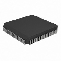
PIC16C924-04I/L Microchip Technology, PIC16C924-04I/L Datasheet - Page 5

PIC16C924-04I/L
Manufacturer Part Number
PIC16C924-04I/L
Description
IC MCU OTP 4KX14 LCD DVR 68PLCC
Manufacturer
Microchip Technology
Series
PIC® 16Cr
Datasheets
1.PIC16F616T-ISL.pdf
(8 pages)
2.PIC16F818-ISO.pdf
(6 pages)
3.PIC16C923-04L.pdf
(189 pages)
4.PIC16LC924-04L.pdf
(10 pages)
Specifications of PIC16C924-04I/L
Core Processor
PIC
Core Size
8-Bit
Speed
4MHz
Connectivity
I²C, SPI
Peripherals
LCD, POR, PWM, WDT
Number Of I /o
25
Program Memory Size
7KB (4K x 14)
Program Memory Type
OTP
Ram Size
176 x 8
Voltage - Supply (vcc/vdd)
4 V ~ 6 V
Data Converters
A/D 5x8b
Oscillator Type
External
Operating Temperature
-40°C ~ 85°C
Package / Case
68-PLCC
Processor Series
PIC16C
Core
PIC
Data Bus Width
8 bit
Data Ram Size
176 B
Interface Type
I2C, SPI
Maximum Clock Frequency
8 MHz
Number Of Programmable I/os
25
Number Of Timers
3
Operating Supply Voltage
2.5 V to 6 V
Maximum Operating Temperature
+ 85 C
Mounting Style
SMD/SMT
3rd Party Development Tools
52715-96, 52716-328, 52717-734
Development Tools By Supplier
ICE2000
Minimum Operating Temperature
- 40 C
On-chip Adc
8 bit, 5 Channel
For Use With
AC164308 - MODULE SKT FOR PM3 68PLCCDVA16XL680 - ADAPTER DEVICE FOR MPLAB-ICEAC164024 - ADAPTER PICSTART PLUS 68PLCCAC164022 - MODULE SKT PROMATEII 68PLCC
Lead Free Status / RoHS Status
Lead free / RoHS Compliant
Eeprom Size
-
Lead Free Status / Rohs Status
Details
Other names
Q701521
Available stocks
Company
Part Number
Manufacturer
Quantity
Price
Company:
Part Number:
PIC16C924-04I/L
Manufacturer:
Microchip Technology
Quantity:
10 000
4. Module: Timer1
FIGURE 1:
5. Module: I/O Ports
TMR1 Increment
Clock (Input to Prescaler)
2001 Microchip Technology Inc.
The operation of Timer1 needs some clarification
when the timer registers are written and the
TMR1ON bit is set.
The internal clock signal that is the input to the
TMR1 prescaler affects the incrementing of Timer1
(TMR1H:TMR1L registers and the Timer1 pres-
caler). When the Timer1 registers are NOT written,
the Timer1 will increment on the rising edge of the
TMR1 increment clock.
When the TMR1H and/or TMR1L registers are
written while this clock is high, TMR1 will incre-
ment on the next rising edge of this clock.
The block diagram for PORTC presented in
Figure 5-5 of the Device Data Sheet (DS30444E)
is incorrect. The correct block diagram is shown in
Figure 2.
Write to TMR1H and/or TMR1L Register(s)
WRITES TO TIMER1 (EXTERNAL CLOCK / OSCILLATOR MODE)
TMR1H:TMR1L Increments
Write to TMR1H and/or TMR1L Register(s)
TMR1H:TMR1L Increments
FIGURE 2:
Note 1: I/O pins have diode protection to V
Peripheral Data Out
Port/Peripheral Select
Data Bus
OE
Peripheral
Peripheral Input
WR
TRIS
WR
Port
When the TMR1H and/or TMR1L registers are
written while this clock is low, TMR1 will not incre-
ment on the next rising edge of this clock, but must
first have a falling clock and then the rising clock
for TMR1 to increment.
Figure 1 shows the two cases of writes to the
TMR1H and/or TMR1L registers. Due to the V
and V
external Timer1 oscillator components, and exter-
nal clock frequency, the Timer1 increment clock
may not be of a 50% duty cycle.
The TMR1 increment clock is out of phase of the
T1OSO/T1CKI pin by a small propagation delay.
(3)
2: Port/Peripheral select signal selects between
3: Peripheral OE (output enable) is only activated if
port data and peripheral output.
peripheral select is active.
IL
RD
Port
TRIS Latch
Data Latch
thresholds on the oscillator/clock pins,
D
D
CK
CK
RD TRIS
PORTC BLOCK DIAGRAM
(PERIPHERAL OUTPUT
OVERRIDE)
Q
Q
Q
Q
(2)
PIC16C924
0
1
Q
EN
D
DS80111B-page 5
Schmitt
Trigger
DD
V
V
N
P
SS
and V
DD
I/O
pin
SS
(1)
.
IH


