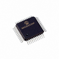
PIC16F874-04/PQ Microchip Technology, PIC16F874-04/PQ Datasheet - Page 33

PIC16F874-04/PQ
Manufacturer Part Number
PIC16F874-04/PQ
Description
IC MCU FLASH 4KX14 EE 44MQFP
Manufacturer
Microchip Technology
Series
PIC® 16Fr
Datasheets
1.PIC16F616T-ISL.pdf
(8 pages)
2.PIC16F688T-ISL.pdf
(688 pages)
3.PIC16F873-04SO.pdf
(218 pages)
4.PIC16F873-04SO.pdf
(5 pages)
5.PIC16F873-04SO.pdf
(5 pages)
Specifications of PIC16F874-04/PQ
Core Size
8-Bit
Program Memory Size
7KB (4K x 14)
Oscillator Type
External
Core Processor
PIC
Speed
4MHz
Connectivity
I²C, SPI, UART/USART
Peripherals
Brown-out Detect/Reset, POR, PWM, WDT
Number Of I /o
33
Program Memory Type
FLASH
Eeprom Size
128 x 8
Ram Size
192 x 8
Voltage - Supply (vcc/vdd)
4 V ~ 5.5 V
Data Converters
A/D 8x10b
Operating Temperature
0°C ~ 70°C
Package / Case
44-MQFP, 44-PQFP
Controller Family/series
PIC16F
No. Of I/o's
33
Eeprom Memory Size
128Byte
Ram Memory Size
192Byte
Cpu Speed
4MHz
Processor Series
PIC16F
Core
PIC
Data Bus Width
8 bit
Data Ram Size
192 B
Interface Type
MSSP, PSP, USART
Maximum Clock Frequency
20 MHz
Number Of Programmable I/os
33
Number Of Timers
3 bit
Operating Supply Voltage
2 V to 5.5 V
Maximum Operating Temperature
+ 70 C
Mounting Style
SMD/SMT
3rd Party Development Tools
52715-96, 52716-328, 52717-734
Development Tools By Supplier
PG164130, DV164035, DV244005, DV164005, PG164120, ICE2000, DM163022, DV164120
Minimum Operating Temperature
0 C
On-chip Adc
8
Lead Free Status / RoHS Status
Lead free / RoHS Compliant
Lead Free Status / RoHS Status
Lead free / RoHS Compliant, Lead free / RoHS Compliant
Available stocks
Company
Part Number
Manufacturer
Quantity
Price
Company:
Part Number:
PIC16F874-04/PQ
Manufacturer:
MICROCHIP
Quantity:
9 100
Company:
Part Number:
PIC16F874-04/PQ
Manufacturer:
Microchip Technology
Quantity:
10 000
3.2
PORTB is an 8-bit wide, bi-directional port. The corre-
sponding data direction register is TRISB. Setting a
TRISB bit (= 1) will make the corresponding PORTB pin
an input (i.e., put the corresponding output driver in a
Hi-Impedance mode). Clearing a TRISB bit (= 0) will
make the corresponding PORTB pin an output (i.e., put
the contents of the output latch on the selected pin).
Three pins of PORTB are multiplexed with the Low
Voltage Programming function: RB3/PGM, RB6/PGC
and RB7/PGD. The alternate functions of these pins
are described in the Special Features Section.
Each of the PORTB pins has a weak internal pull-up. A
single control bit can turn on all the pull-ups. This is per-
formed by clearing bit RBPU (OPTION_REG<7>). The
weak pull-up is automatically turned off when the port
pin is configured as an output. The pull-ups are dis-
abled on a Power-on Reset.
FIGURE 3-3:
Four of the PORTB pins, RB7:RB4, have an interrupt-
on-change feature. Only pins configured as inputs can
cause this interrupt to occur (i.e., any RB7:RB4 pin
configured as an output is excluded from the interrupt-
on-change comparison). The input pins (of RB7:RB4)
are compared with the old value latched on the last
read of PORTB. The “mismatch” outputs of RB7:RB4
are OR’ed together to generate the RB Port Change
Interrupt with flag bit RBIF (INTCON<0>).
2001 Microchip Technology Inc.
Note 1: I/O pins have diode protection to V
RBPU
Data Bus
WR Port
WR TRIS
RD TRIS
RD Port
RB0/INT
RB3/PGM
2: To enable weak pull-ups, set the appropriate TRIS
(2)
PORTB and the TRISB Register
bit(s) and clear the RBPU bit (OPTION_REG<7>).
Data Latch
TRIS Latch
D
D
CK
CK
Schmitt Trigger
Buffer
BLOCK DIAGRAM OF
RB3:RB0 PINS
Q
Q
Q
EN
TTL
Input
Buffer
DD
D
and V
V
RD Port
P
DD
SS
Weak
Pull-up
.
I/O
pin
(1)
This interrupt can wake the device from SLEEP. The
user, in the Interrupt Service Routine, can clear the
interrupt in the following manner:
a)
b)
A mismatch condition will continue to set flag bit RBIF.
Reading PORTB will end the mismatch condition and
allow flag bit RBIF to be cleared.
The interrupt-on-change feature is recommended for
wake-up on key depression operation and operations
where PORTB is only used for the interrupt-on-change
feature. Polling of PORTB is not recommended while
using the interrupt-on-change feature.
This interrupt-on-mismatch feature, together with soft-
ware configureable pull-ups on these four pins, allow
easy interface to a keypad and make it possible for
wake-up on key depression. Refer to the Embedded
Control Handbook, “Implementing Wake-up on Key
Strokes” (AN552).
RB0/INT is an external interrupt input pin and is config-
ured using the INTEDG bit (OPTION_REG<6>).
RB0/INT is discussed in detail in Section 12.10.1.
FIGURE 3-4:
RBPU
Data Bus
WR Port
WR TRIS
RD TRIS
RD Port
Set RBIF
RB7:RB6
In Serial Programming Mode
Note 1: I/O pins have diode protection to V
Any read or write of PORTB. This will end the
mismatch condition.
Clear flag bit RBIF.
From other
RB7:RB4 pins
(2)
2: To enable weak pull-ups, set the appropriate TRIS
bit(s) and clear the RBPU bit (OPTION_REG<7>).
TRIS Latch
Data Latch
D
D
CK
CK
Q
Q
BLOCK DIAGRAM OF
RB7:RB4 PINS
PIC16F87X
Q
Q
Latch
EN
EN
D
D
DS30292C-page 31
TTL
Input
Buffer
DD
and V
V
P
DD
Weak
Pull-up
RD Port
SS
Buffer
I/O
pin
.
Q1
Q3
ST
(1)


