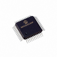
PIC16F874-04/PQ Microchip Technology, PIC16F874-04/PQ Datasheet - Page 45

PIC16F874-04/PQ
Manufacturer Part Number
PIC16F874-04/PQ
Description
IC MCU FLASH 4KX14 EE 44MQFP
Manufacturer
Microchip Technology
Series
PIC® 16Fr
Datasheets
1.PIC16F616T-ISL.pdf
(8 pages)
2.PIC16F688T-ISL.pdf
(688 pages)
3.PIC16F873-04SO.pdf
(218 pages)
4.PIC16F873-04SO.pdf
(5 pages)
5.PIC16F873-04SO.pdf
(5 pages)
Specifications of PIC16F874-04/PQ
Core Size
8-Bit
Program Memory Size
7KB (4K x 14)
Oscillator Type
External
Core Processor
PIC
Speed
4MHz
Connectivity
I²C, SPI, UART/USART
Peripherals
Brown-out Detect/Reset, POR, PWM, WDT
Number Of I /o
33
Program Memory Type
FLASH
Eeprom Size
128 x 8
Ram Size
192 x 8
Voltage - Supply (vcc/vdd)
4 V ~ 5.5 V
Data Converters
A/D 8x10b
Operating Temperature
0°C ~ 70°C
Package / Case
44-MQFP, 44-PQFP
Controller Family/series
PIC16F
No. Of I/o's
33
Eeprom Memory Size
128Byte
Ram Memory Size
192Byte
Cpu Speed
4MHz
Processor Series
PIC16F
Core
PIC
Data Bus Width
8 bit
Data Ram Size
192 B
Interface Type
MSSP, PSP, USART
Maximum Clock Frequency
20 MHz
Number Of Programmable I/os
33
Number Of Timers
3 bit
Operating Supply Voltage
2 V to 5.5 V
Maximum Operating Temperature
+ 70 C
Mounting Style
SMD/SMT
3rd Party Development Tools
52715-96, 52716-328, 52717-734
Development Tools By Supplier
PG164130, DV164035, DV244005, DV164005, PG164120, ICE2000, DM163022, DV164120
Minimum Operating Temperature
0 C
On-chip Adc
8
Lead Free Status / RoHS Status
Lead free / RoHS Compliant
Lead Free Status / RoHS Status
Lead free / RoHS Compliant, Lead free / RoHS Compliant
Available stocks
Company
Part Number
Manufacturer
Quantity
Price
Company:
Part Number:
PIC16F874-04/PQ
Manufacturer:
MICROCHIP
Quantity:
9 100
Company:
Part Number:
PIC16F874-04/PQ
Manufacturer:
Microchip Technology
Quantity:
10 000
4.2
Reading EEPROM data memory only requires that the
desired address to access be written to the EEADR
register and clear the EEPGD bit. After the RD bit is set,
data will be available in the EEDATA register on the
very next instruction cycle. EEDATA will hold this value
until another read operation is initiated or until it is writ-
ten by firmware.
The steps to reading the EEPROM data memory are:
1.
2.
3.
4.
EXAMPLE 4-1:
4.3
There are many steps in writing to the EEPROM data
memory. Both address and data values must be written
to the SFRs. The EEPGD bit must be cleared, and the
WREN bit must be set, to enable writes. The WREN bit
should be kept clear at all times, except when writing to
the EEPROM data. The WR bit can only be set if the
WREN bit was set in a previous operation, i.e., they
both cannot be set in the same operation. The WREN
bit should then be cleared by firmware after the write.
Clearing the WREN bit before the write actually com-
pletes will not terminate the write in progress.
Writes to EEPROM data memory must also be pref-
aced with a special sequence of instructions, that pre-
vent inadvertent write operations. This is a sequence of
five instructions that must be executed without interrup-
tions. The firmware should verify that a write is not in
progress, before starting another cycle.
BSF
BCF
MOVF
MOVWF
BSF
BCF
BSF
BCF
MOVF
2001 Microchip Technology Inc.
Write the address to EEDATA. Make sure that
the address is not larger than the memory size
of the PIC16F87X device.
Clear the EEPGD bit to point to EEPROM data
memory.
Set the RD bit to start the read operation.
Read the data from the EEDATA register.
Reading the EEPROM Data
Memory
Writing to the EEPROM Data
Memory
STATUS, RP1
STATUS, RP0
ADDR, W
EEADR
STATUS, RP0
EECON1, EEPGD
EECON1, RD
STATUS, RP0
EEDATA, W
EEPROM DATA READ
;
;Bank 2
;Write address
;to read from
;Bank 3
;Point to Data memory
;Start read operation
;Bank 2
;W = EEDATA
The steps to write to EEPROM data memory are:
1.
2.
3.
4.
5.
6.
7.
8.
9.
10. At the completion of the write cycle, the WR bit
EXAMPLE 4-2:
BSF
BSF
BTFSC
GOTO
BCF
MOVF
MOVWF
MOVF
MOVWF
BSF
BCF
BSF
BCF
MOVLW
MOVWF
MOVLW
MOVWF
BSF
BSF
BCF
If step 10 is not implemented, check the WR bit
to see if a write is in progress.
Write the address to EEADR. Make sure that the
address is not larger than the memory size of
the PIC16F87X device.
Write the 8-bit data value to be programmed in
the EEDATA register.
Clear the EEPGD bit to point to EEPROM data
memory.
Set the WREN bit to enable program operations.
Disable interrupts (if enabled).
Execute the special five instruction sequence:
• Write 55h to EECON2 in two steps (first to W,
• Write AAh to EECON2 in two steps (first to
• Set the WR bit
Enable interrupts (if using interrupts).
Clear the WREN bit to disable program opera-
tions.
is cleared and the EEIF interrupt flag bit is set.
(EEIF must be cleared by firmware.) If step 1 is
not implemented, then firmware should check
for EEIF to be set, or WR to clear, to indicate the
end of the program cycle.
then to EECON2)
W, then to EECON2)
STATUS, RP1
STATUS, RP0
EECON1, WR
$-1
STATUS, RP0
ADDR, W
EEADR
VALUE, W
EEDATA
STATUS, RP0
EECON1, EEPGD ;Point to Data memory
EECON1, WREN
INTCON, GIE
0x55
EECON2
0xAA
EECON2
EECON1, WR
INTCON, GIE
EECON1, WREN
EEPROM DATA WRITE
PIC16F87X
;Only disable interrupts
;
;Bank 3
;Wait for
;write to finish
;Bank 2
;Address to
;write to
;Data to
;write
;Bank 3
;Enable writes
;if already enabled,
;otherwise discard
;Write 55h to
;EECON2
;Write AAh to
;EECON2
;Start write operation
;Only enable interrupts
;if using interrupts,
;otherwise discard
;Disable writes
DS30292C-page 43


