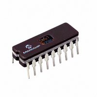
PIC16C56A/JW Microchip Technology, PIC16C56A/JW Datasheet - Page 39

PIC16C56A/JW
Manufacturer Part Number
PIC16C56A/JW
Description
IC MCU EPROM 1KX12 18CDIP
Manufacturer
Microchip Technology
Series
PIC® 16Cr
Specifications of PIC16C56A/JW
Core Processor
PIC
Core Size
8-Bit
Speed
20MHz
Peripherals
POR, WDT
Number Of I /o
12
Program Memory Size
1.5KB (1K x 12)
Program Memory Type
EPROM, UV
Ram Size
25 x 8
Voltage - Supply (vcc/vdd)
3 V ~ 5.5 V
Oscillator Type
External
Operating Temperature
0°C ~ 70°C
Package / Case
18-CDIP (0.300", 7.62mm) Window
Lead Free Status / RoHS Status
Contains lead / RoHS non-compliant
Eeprom Size
-
Data Converters
-
Connectivity
-
Available stocks
Company
Part Number
Manufacturer
Quantity
Price
Company:
Part Number:
PIC16C56A/JW
Manufacturer:
Microchip Technology
Quantity:
2
- Current page: 39 of 194
- Download datasheet (3Mb)
8.0
The Timer0 module has the following features:
• 8-bit timer/counter register, TMR0
• 8-bit software programmable prescaler
• Internal or external clock select
Figure 8-1 is a simplified block diagram of the Timer0
module, while Figure 8-2 shows the electrical structure
of the Timer0 input.
Timer mode is selected by clearing the T0CS bit
(OPTION<5>). In Timer mode, the Timer0 module will
increment every instruction cycle (without prescaler). If
TMR0 register is written, the increment is inhibited for
the following two cycles (Figure 8-3 and Figure 8-4).
The user can work around this by writing an adjusted
value to the TMR0 register.
FIGURE 8-1:
FIGURE 8-2:
- Readable and writable
- Edge select for external clock
2002 Microchip Technology Inc.
TIMER0 MODULE AND TMR0
REGISTER
T0CKI
Note 1: Bits T0CS, T0SE, PSA, PS2, PS1 and PS0 are located in the OPTION register
pin
2: The prescaler is shared with the Watchdog Timer (Figure 8-6).
T0SE
(Section 6.4).
TIMER0 BLOCK DIAGRAM
ELECTRICAL STRUCTURE OF T0CKI PIN
F
(1)
OSC
/4
T0CKI
T0CS
pin
Note 1: ESD protection circuits.
0
1
(1)
V
SS
PS2, PS1, PS0
(1)
Programmable
Prescaler
Preliminary
V
SS
3
N
(2)
(1)
(1)
R
IN
Counter mode is selected by setting the T0CS bit
(OPTION<5>). In this mode, Timer0 will increment
either on every rising or falling edge of pin T0CKI. The
incrementing edge is determined by the source edge
select bit T0SE (OPTION<4>). Clearing the T0SE bit
selects the rising edge. Restrictions on the external
clock input are discussed in detail in Section 8.1.
The prescaler assignment is controlled in software by
the control bit PSA (OPTION<3>). Clearing the PSA bit
will assign the prescaler to Timer0. The prescaler is not
readable or writable. When the prescaler is assigned to
the Timer0 module, prescale values of 1:2, 1:4,...,
1:256 are selectable. Section 8.2 details the operation
of the prescaler.
A summary of registers associated with the Timer0
module is found in Table 8-1.
PSA
Note:
1
0
(1)
PSout
Schmitt Trigger
Input Buffer
The prescaler may be used by either the
Timer0 module or the Watchdog Timer, but
not both.
(2 cycle delay)
Sync with
Internal
Clocks
PSout
Sync
PIC16C5X
TMR0 reg
Data Bus
DS30453D-page 37
8
Related parts for PIC16C56A/JW
Image
Part Number
Description
Manufacturer
Datasheet
Request
R

Part Number:
Description:
Manufacturer:
Microchip Technology Inc.
Datasheet:

Part Number:
Description:
IC MCU OTP 1KX12 18SOIC
Manufacturer:
Microchip Technology
Datasheet:

Part Number:
Description:
IC MCU OTP 1KX12 18DIP
Manufacturer:
Microchip Technology
Datasheet:

Part Number:
Description:
IC MCU OTP 1KX12 18DIP
Manufacturer:
Microchip Technology
Datasheet:

Part Number:
Description:
IC MCU OTP 1KX12 18DIP
Manufacturer:
Microchip Technology
Datasheet:

Part Number:
Description:
IC MCU OTP 1KX12 18DIP
Manufacturer:
Microchip Technology
Datasheet:

Part Number:
Description:
IC MCU OTP 1KX12 18SOIC
Manufacturer:
Microchip Technology
Datasheet:

Part Number:
Description:
IC MCU OTP 1KX12 18DIP
Manufacturer:
Microchip Technology
Datasheet:

Part Number:
Description:
IC MCU OTP 1KX12 18SOIC
Manufacturer:
Microchip Technology
Datasheet:

Part Number:
Description:
IC MCU OTP 1KX12 20SSOP
Manufacturer:
Microchip Technology
Datasheet:

Part Number:
Description:
IC MCU OTP 1KX12 20SSOP
Manufacturer:
Microchip Technology
Datasheet:

Part Number:
Description:
IC MCU OTP 1KX12 18SOIC
Manufacturer:
Microchip Technology
Datasheet:

Part Number:
Description:
IC MCU OTP 1KX12 18DIP
Manufacturer:
Microchip Technology
Datasheet:

Part Number:
Description:
IC MCU OTP 1KX12 18DIP
Manufacturer:
Microchip Technology
Datasheet:

Part Number:
Description:
IC MCU OTP 1KX12 18DIP
Manufacturer:
Microchip Technology
Datasheet:


