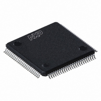
LPC1768FBD100,551 NXP Semiconductors, LPC1768FBD100,551 Datasheet - Page 23

LPC1768FBD100,551
Manufacturer Part Number
LPC1768FBD100,551
Description
IC ARM CORTEX MCU 512K 100-LQFP
Manufacturer
NXP Semiconductors
Series
LPC17xxr
Datasheets
1.OM11043.pdf
(79 pages)
2.LPC1765FBD100551.pdf
(74 pages)
3.LPC1769FBD100551.pdf
(66 pages)
Specifications of LPC1768FBD100,551
Program Memory Type
FLASH
Program Memory Size
512KB (512K x 8)
Package / Case
100-LQFP
Core Processor
ARM® Cortex-M3™
Core Size
32-Bit
Speed
100MHz
Connectivity
CAN, Ethernet, I²C, IrDA, Microwire, SPI, SSI, UART/USART, USB OTG
Peripherals
Brown-out Detect/Reset, DMA, I²S, Motor Control PWM, POR, PWM, WDT
Number Of I /o
70
Ram Size
64K x 8
Voltage - Supply (vcc/vdd)
2.4 V ~ 3.6 V
Data Converters
A/D 8x12b, D/A 1x10b
Oscillator Type
Internal
Operating Temperature
-40°C ~ 85°C
Processor Series
LPC17
Core
ARM Cortex M3
Data Bus Width
32 bit
Data Ram Size
64 KB
Interface Type
CAN, I2C, SPI, UART
Maximum Clock Frequency
100 MHz
Number Of Programmable I/os
70
Number Of Timers
3
Operating Supply Voltage
3.3 V
Maximum Operating Temperature
+ 85 C
Mounting Style
SMD/SMT
3rd Party Development Tools
MDK-ARM, RL-ARM, ULINK2, MCB1760, MCB1760U, MCB1760UME, IRD-LPC1768-DEV, KSK-LPC1768-JL
Development Tools By Supplier
OM11032, OM11033, OM11034, OM11035, OM11043
Minimum Operating Temperature
- 40 C
On-chip Adc
12 bit, 8 Channel
On-chip Dac
10 bit
Package
100LQFP
Device Core
ARM Cortex M3
Family Name
LPC17xx
Maximum Speed
100 MHz
Cpu Family
LPC17xx
Device Core Size
32b
Frequency (max)
100MHz
Total Internal Ram Size
64KB
# I/os (max)
70
Number Of Timers - General Purpose
4
Operating Supply Voltage (typ)
3.3V
Operating Supply Voltage (max)
3.6V
Operating Supply Voltage (min)
2.4V
Instruction Set Architecture
RISC
Operating Temp Range
-40C to 85C
Operating Temperature Classification
Industrial
Mounting
Surface Mount
Pin Count
100
Package Type
LQFP
Lead Free Status / RoHS Status
Lead free / RoHS Compliant
For Use With
568-4916 - DEVELOPMENT BOARD LPC1768 MBED568-4816 - EVAL BOARD FOR MCB1768568-4815 - KIT EVAL LPC1768 CR622-1032 - KIT DEV IND REF DESIGN LPC1768622-1005 - USB IN-CIRCUIT PROG ARM7 LPC2K
Eeprom Size
-
Lead Free Status / Rohs Status
Lead free / RoHS Compliant
Other names
568-4796
935288608551
935288608551
Available stocks
Company
Part Number
Manufacturer
Quantity
Price
Company:
Part Number:
LPC1768FBD100,551
Manufacturer:
NXP Semiconductors
Quantity:
10 000
Part Number:
LPC1768FBD100,551
Manufacturer:
NXP/恩智浦
Quantity:
20 000
NXP Semiconductors
LPC1769_68_67_66_65_64_63
Product data sheet
7.10.1 Features
7.11.1 Features
7.11 Ethernet
Additionally, any pin on Port 0 and Port 2 (total of 42 pins) providing a digital function can
be programmed to generate an interrupt on a rising edge, a falling edge, or both. The
edge detection is asynchronous, so it may operate when clocks are not present such as
during Power-down mode. Each enabled interrupt can be used to wake up the chip from
Power-down mode.
Remark: The Ethernet controller is available on parts LPC1769/68/67/66/64. The
Ethernet block supports bus clock rates of up to 100 MHz (LPC1768/67/66/64) or 120
MHz (LPC1769). See
The Ethernet block contains a full featured 10 Mbit/s or 100 Mbit/s Ethernet MAC
designed to provide optimized performance through the use of DMA hardware
acceleration. Features include a generous suite of control registers, half or full duplex
operation, flow control, control frames, hardware acceleration for transmit retry, receive
packet filtering and wake-up on LAN activity. Automatic frame transmission and reception
with scatter-gather DMA off-loads many operations from the CPU.
The Ethernet block and the CPU share the ARM Cortex-M3 D-code and system bus
through the AHB-multilayer matrix to access the various on-chip SRAM blocks for
Ethernet data, control, and status information.
The Ethernet block interfaces between an off-chip Ethernet PHY using the Reduced MII
(RMII) protocol and the on-chip Media Independent Interface Management (MIIM) serial
bus.
•
•
•
•
•
•
Bit level set and clear registers allow a single instruction to set or clear any number of
bits in one port.
Direction control of individual bits.
All I/O default to inputs after reset.
Pull-up/pull-down resistor configuration and open-drain configuration can be
programmed through the pin connect block for each GPIO pin.
Ethernet standards support:
– Supports 10 Mbit/s or 100 Mbit/s PHY devices including 10 Base-T, 100 Base-TX,
– Fully compliant with IEEE standard 802.3.
– Fully compliant with 802.3x full duplex flow control and half duplex back pressure.
– Flexible transmit and receive frame options.
– Virtual Local Area Network (VLAN) frame support.
Memory management:
– Independent transmit and receive buffers memory mapped to shared SRAM.
– DMA managers with scatter/gather DMA and arrays of frame descriptors.
– Memory traffic optimized by buffering and pre-fetching.
100 Base-FX, and 100 Base-T4.
All information provided in this document is subject to legal disclaimers.
Table
Rev. 6.01 — 11 March 2011
2.
LPC1769/68/67/66/65/64/63
32-bit ARM Cortex-M3 microcontroller
© NXP B.V. 2011. All rights reserved.
23 of 79


