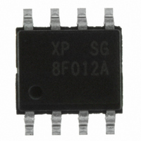
Z8F012ASB020SG Zilog, Z8F012ASB020SG Datasheet - Page 168

Z8F012ASB020SG
Manufacturer Part Number
Z8F012ASB020SG
Description
IC ENCORE XP MCU FLASH 1K 8SOIC
Manufacturer
Zilog
Series
Encore!® XP®r
Datasheet
1.Z8F011ASB020EG.pdf
(282 pages)
Specifications of Z8F012ASB020SG
Core Processor
Z8
Core Size
8-Bit
Speed
20MHz
Connectivity
IrDA, UART/USART
Peripherals
Brown-out Detect/Reset, LED, LVD, POR, PWM, Temp Sensor, WDT
Number Of I /o
6
Program Memory Size
1KB (1K x 8)
Program Memory Type
FLASH
Eeprom Size
16 x 8
Ram Size
256 x 8
Voltage - Supply (vcc/vdd)
2.7 V ~ 3.6 V
Data Converters
A/D 4x10b
Oscillator Type
Internal
Operating Temperature
0°C ~ 70°C
Package / Case
8-SOIC (3.9mm Width)
Processor Series
Z8F012Ax
Core
eZ8
Data Bus Width
8 bit
Data Ram Size
256 B
Interface Type
UART
Maximum Clock Frequency
20 MHz
Number Of Programmable I/os
6
Number Of Timers
2
Operating Supply Voltage
2.7 V to 3.6 V
Maximum Operating Temperature
+ 70 C
Mounting Style
SMD/SMT
Development Tools By Supplier
Z8F04A08100KITG, Z8F04A28100KITG, ZENETSC0100ZACG, ZENETSC0100ZACG, ZUSBOPTSC01ZACG, ZUSBSC00100ZAC, ZUSBSC00100ZACG
Minimum Operating Temperature
0 C
On-chip Adc
10 bit, 4 Channel
Lead Free Status / RoHS Status
Lead free / RoHS Compliant
Other names
269-4039
Z8F012ASB020SG
Z8F012ASB020SG
- Current page: 168 of 282
- Download datasheet (4Mb)
®
Z8 Encore! XP
F082A Series
Product Specification
157
1 = Watchdog Timer is enabled upon execution of the WDT instruction. Once enabled, the
Watchdog Timer can only be disabled by a Reset or Stop Mode Recovery. This setting is
the default for unprogrammed (erased) Flash.
OSC_SEL[1:0]—Oscillator Mode Selection
00 = On-chip oscillator configured for use with external RC networks (<4 MHz).
01 = Minimum power for use with very low frequency crystals (32 kHz to 1.0 MHz).
10 = Medium power for use with medium frequency crystals or ceramic resonators (0.5
MHz to 5.0 MHz).
11 = Maximum power for use with high frequency crystals (5.0 MHz to 20.0 MHz). This
setting is the default for unprogrammed (erased) Flash.
VBO_AO—Voltage Brownout Protection Always On
0 = Voltage Brownout Protection can be disabled in STOP mode to reduce total power
consumption. For the block to be disabled, the power control register bit must also be writ-
ten (see
Power Control Register Definitions
on page 34).
1 = Voltage Brownout Protection is always enabled including during STOP mode. This
setting is the default for unprogrammed (erased) Flash.
FRP—Flash Read Protect
0 = User program code is inaccessible. Limited control features are available through the
On-Chip Debugger.
1 = User program code is accessible. All On-Chip Debugger commands are enabled. This
setting is the default for unprogrammed (erased) Flash.
Reserved—Must be 1.
FWP—Flash Write Protect
This Option Bit provides Flash Program Memory protection:
0 = Programming and erasure disabled for all of Flash Program Memory. Programming,
Page Erase, and Mass Erase through User Code is disabled. Mass Erase is available using
the On-Chip Debugger.
1 = Programming, Page Erase, and Mass Erase are enabled for all of Flash program
memory.
PS022825-0908
Flash Option Bits
Related parts for Z8F012ASB020SG
Image
Part Number
Description
Manufacturer
Datasheet
Request
R

Part Number:
Description:
Communication Controllers, ZILOG INTELLIGENT PERIPHERAL CONTROLLER (ZIP)
Manufacturer:
Zilog, Inc.
Datasheet:

Part Number:
Description:
KIT DEV FOR Z8 ENCORE 16K TO 64K
Manufacturer:
Zilog
Datasheet:

Part Number:
Description:
KIT DEV Z8 ENCORE XP 28-PIN
Manufacturer:
Zilog
Datasheet:

Part Number:
Description:
DEV KIT FOR Z8 ENCORE 8K/4K
Manufacturer:
Zilog
Datasheet:

Part Number:
Description:
KIT DEV Z8 ENCORE XP 28-PIN
Manufacturer:
Zilog
Datasheet:

Part Number:
Description:
DEV KIT FOR Z8 ENCORE 4K TO 8K
Manufacturer:
Zilog
Datasheet:

Part Number:
Description:
CMOS Z8 microcontroller. ROM 16 Kbytes, RAM 256 bytes, speed 16 MHz, 32 lines I/O, 3.0V to 5.5V
Manufacturer:
Zilog, Inc.
Datasheet:

Part Number:
Description:
Low-cost microcontroller. 512 bytes ROM, 61 bytes RAM, 8 MHz
Manufacturer:
Zilog, Inc.
Datasheet:

Part Number:
Description:
Z8 4K OTP Microcontroller
Manufacturer:
Zilog, Inc.
Datasheet:

Part Number:
Description:
CMOS SUPER8 ROMLESS MCU
Manufacturer:
Zilog, Inc.
Datasheet:

Part Number:
Description:
SL1866 CMOSZ8 OTP Microcontroller
Manufacturer:
Zilog, Inc.
Datasheet:

Part Number:
Description:
SL1866 CMOSZ8 OTP Microcontroller
Manufacturer:
Zilog, Inc.
Datasheet:

Part Number:
Description:
OTP (KB) = 1, RAM = 125, Speed = 12, I/O = 14, 8-bit Timers = 2, Comm Interfaces Other Features = Por, LV Protect, Voltage = 4.5-5.5V
Manufacturer:
Zilog, Inc.
Datasheet:

Part Number:
Description:
Manufacturer:
Zilog, Inc.
Datasheet:


