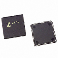
Z8F2422VS020SG Zilog, Z8F2422VS020SG Datasheet - Page 196

Z8F2422VS020SG
Manufacturer Part Number
Z8F2422VS020SG
Description
IC ENCORE MCU FLASH 24K 68PLCC
Manufacturer
Zilog
Series
Encore!® XP®r
Specifications of Z8F2422VS020SG
Core Processor
Z8
Core Size
8-Bit
Speed
20MHz
Connectivity
I²C, IrDA, SPI, UART/USART
Peripherals
Brown-out Detect/Reset, DMA, POR, PWM, WDT
Number Of I /o
46
Program Memory Size
24KB (24K x 8)
Program Memory Type
FLASH
Ram Size
2K x 8
Voltage - Supply (vcc/vdd)
3 V ~ 3.6 V
Data Converters
A/D 12x10b
Oscillator Type
Internal
Operating Temperature
0°C ~ 70°C
Package / Case
68-LCC (J-Lead)
Processor Series
Z8F242x
Core
eZ8
Data Bus Width
8 bit
Data Ram Size
2 KB
Interface Type
I2C, SPI, UART
Maximum Clock Frequency
20 MHz
Number Of Programmable I/os
46
Number Of Timers
4
Operating Supply Voltage
3 V to 3.6 V
Maximum Operating Temperature
+ 70 C
Mounting Style
SMD/SMT
Development Tools By Supplier
Z8F64200100KITG, ZENETSC0100ZACG, ZUSBSC00100ZACG, Z8F64210100ZDA, Z8F64210100ZDP, Z8F64210100ZDV, Z8F64220100ZDA, Z8F64220100ZDV, Z8F6422AR00ZEM, Z8F6422VS00ZEM, Z8F6421AN00ZEM
Minimum Operating Temperature
0 C
On-chip Adc
10 bit, 12 Channel
Lead Free Status / RoHS Status
Lead free / RoHS Compliant
Eeprom Size
-
Lead Free Status / Rohs Status
Details
Other names
269-4253
Z8F2422VS020SG
Z8F2422VS020SG
Available stocks
Company
Part Number
Manufacturer
Quantity
Price
- Current page: 196 of 297
- Download datasheet (9Mb)
PS019921-0308
Caution:
Flash Read Protection
Flash Write/Erase Protection
Timing Using the Flash Frequency Registers
Before performing a program or erase operation on the Flash memory, you must first
configure the Flash Frequency High and Low Byte registers. The Flash Frequency
registers allow programming and erasure of the Flash with system clock frequencies
ranging from 20 kHz through 20 MHz (the valid range is limited to the device operating
frequencies).
The Flash Frequency High and Low Byte registers combine to form a 16-bit value,
FFREQ, to control timing for Flash program and erase operations. The 16-bit Flash
Frequency value must contain the system clock frequency in kHz. This value is calculated
using the following equation:.
The user code contained within the Flash memory can be protected from external access.
Programming the Flash Read Protect Option Bit prevents reading of user code by the On-
Chip Debugger or by using the Flash Controller Bypass mode. For more information, see
Option Bits
The Z8 Encore! XP
tal program and erasure of the Flash memory contents. This protection is provided by the
Flash Controller unlock mechanism, the Flash Sector Protect register, and the Flash Write
Protect option bit.
Flash Controller Unlock Mechanism
At Reset, the Flash Controller locks to prevent accidental program or erasure of the Flash
memory. To program or erase the Flash memory, the Flash controller must be unlocked.
After unlocking the Flash Controller, the Flash can be programmed or erased. Any value
written by user code to the Flash Control register or Page Select Register out of sequence
will lock the Flash Controller.
Follow the steps below to unlock the Flash Controller from user code:
1. Write 00H to the Flash Control register to reset the Flash Controller.
2. Write the page to be programmed or erased to the Page Select register.
Flash programming and erasure are not supported for system clock frequencies
below 20 kHz, above 20 MHz, or outside of the device operating frequency
range. The Flash Frequency High and Low Byte registers must be loaded with
the correct value to insure proper Flash programming and erase operations.
on page 191 and
FFREQ[15:0]
®
F64XX Series provides several levels of protection against acciden-
=
On-Chip Debugger
System Clock Frequency (Hz)
------------------------------------------------------------------------
1000
on page 195.
Z8 Encore! XP
Product Specification
®
F64XX Series
Flash Memory
182
Related parts for Z8F2422VS020SG
Image
Part Number
Description
Manufacturer
Datasheet
Request
R

Part Number:
Description:
Communication Controllers, ZILOG INTELLIGENT PERIPHERAL CONTROLLER (ZIP)
Manufacturer:
Zilog, Inc.
Datasheet:

Part Number:
Description:
KIT DEV FOR Z8 ENCORE 16K TO 64K
Manufacturer:
Zilog
Datasheet:

Part Number:
Description:
KIT DEV Z8 ENCORE XP 28-PIN
Manufacturer:
Zilog
Datasheet:

Part Number:
Description:
DEV KIT FOR Z8 ENCORE 8K/4K
Manufacturer:
Zilog
Datasheet:

Part Number:
Description:
KIT DEV Z8 ENCORE XP 28-PIN
Manufacturer:
Zilog
Datasheet:

Part Number:
Description:
DEV KIT FOR Z8 ENCORE 4K TO 8K
Manufacturer:
Zilog
Datasheet:

Part Number:
Description:
CMOS Z8 microcontroller. ROM 16 Kbytes, RAM 256 bytes, speed 16 MHz, 32 lines I/O, 3.0V to 5.5V
Manufacturer:
Zilog, Inc.
Datasheet:

Part Number:
Description:
Low-cost microcontroller. 512 bytes ROM, 61 bytes RAM, 8 MHz
Manufacturer:
Zilog, Inc.
Datasheet:

Part Number:
Description:
Z8 4K OTP Microcontroller
Manufacturer:
Zilog, Inc.
Datasheet:

Part Number:
Description:
CMOS SUPER8 ROMLESS MCU
Manufacturer:
Zilog, Inc.
Datasheet:

Part Number:
Description:
SL1866 CMOSZ8 OTP Microcontroller
Manufacturer:
Zilog, Inc.
Datasheet:

Part Number:
Description:
SL1866 CMOSZ8 OTP Microcontroller
Manufacturer:
Zilog, Inc.
Datasheet:

Part Number:
Description:
OTP (KB) = 1, RAM = 125, Speed = 12, I/O = 14, 8-bit Timers = 2, Comm Interfaces Other Features = Por, LV Protect, Voltage = 4.5-5.5V
Manufacturer:
Zilog, Inc.
Datasheet:

Part Number:
Description:
Manufacturer:
Zilog, Inc.
Datasheet:


