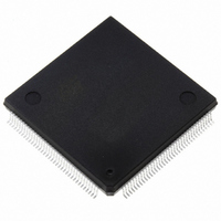
ST10F276Z5Q3 STMicroelectronics, ST10F276Z5Q3 Datasheet - Page 208

ST10F276Z5Q3
Manufacturer Part Number
ST10F276Z5Q3
Description
MCU 16BIT 832KB FLASH 144-PQFP
Manufacturer
STMicroelectronics
Series
ST10r
Datasheet
1.ST10F276Z5T3.pdf
(239 pages)
Specifications of ST10F276Z5Q3
Core Processor
ST10
Core Size
16-Bit
Speed
64MHz
Connectivity
ASC, CAN, EBI/EMI, I²C, SSC, UART/USART
Peripherals
POR, PWM, WDT
Number Of I /o
111
Program Memory Size
832KB (832K x 8)
Program Memory Type
FLASH
Ram Size
68K x 8
Voltage - Supply (vcc/vdd)
4.5 V ~ 5.5 V
Data Converters
A/D 24x10b
Oscillator Type
Internal
Operating Temperature
-40°C ~ 125°C
Package / Case
144-QFP
Processor Series
ST10F27x
Core
ST10
Data Bus Width
16 bit
Data Ram Size
68 KB
Interface Type
CAN/I2C
Maximum Clock Frequency
64 MHz
Number Of Programmable I/os
111
Number Of Timers
5
Operating Supply Voltage
4.5 V to 5.5 V
Maximum Operating Temperature
+ 125 C
Mounting Style
SMD/SMT
Minimum Operating Temperature
- 40 C
On-chip Adc
24-ch x 10-bit
For Use With
497-6399 - KIT DEV STARTER ST10F276Z5
Lead Free Status / RoHS Status
Lead free / RoHS Compliant
Eeprom Size
-
Lead Free Status / Rohs Status
Lead free / RoHS Compliant
Other names
497-5580
Available stocks
Company
Part Number
Manufacturer
Quantity
Price
Company:
Part Number:
ST10F276Z5Q3
Manufacturer:
AD
Quantity:
230
Company:
Part Number:
ST10F276Z5Q3
Manufacturer:
STMicroelectronics
Quantity:
10 000
Company:
Part Number:
ST10F276Z5Q3TR
Manufacturer:
STMicroelectronics
Quantity:
10 000
- Current page: 208 of 239
- Download datasheet (3Mb)
Electrical characteristics
23.8.18
Table 106. Multiplexed bus
208/239
t
t
t
t
t
t
t
t
t
t
t
t
t
t
t
t
t
t
t
5
6
7
8
9
10
11
12
13
14
15
16
17
18
19
22
23
25
27
Symbol
CC
CC
CC
CC
CC
CC
CC
CC
CC
SR
SR
SR
SR
SR
SR
CC
CC
CC
CC
ALE high time
Address setup to ALE
Address hold after ALE
ALE falling edge to RD,
WR (with RW-delay)
ALE falling edge to RD,
WR
(no RW-delay)
Address float after RD, WR
(with RW-delay)
Address float after RD, WR
(no RW-delay)1
RD, WR low time
(with RW-delay)
RD, WR low time
RD to valid data in
RD to valid data in
ALE low to valid data in
Address/Unlatched CS to
valid data in
Data hold after RD
rising edge
Data float after RD1
Data valid to WR
Data hold after WR
ALE rising edge after RD,
WR
Address/Unlatched CS
hold after RD, WR
(no RW-delay)
(with RW-delay)
(no RW-delay)
Multiplexed bus
V
ALE cycle time = 6 TCL + 2t
DD
= 5 V ±10%, V
Parameter
(1)
SS
= 0 V, T
– 8.5 + t
15.5 + t
1.5 + t
28 + t
10 + t
15 + t
10 + t
4 + t
4 + t
4 + t
4 + t
Min.
A
–
–
0
–
F
A
+ t
TCL = 12.5 ns
A
A
A
F
CPU
C
C
F
F
A
= –40 to +125 °C, C
C
A
C
+ t
= 40 MHz
F
20 + 2t
18.5 + t
16.5 + t
+ t
(75 ns at 40 MHz CPU clock without wait states).
17.5 +
Max.
6 + t
18.5
+ t
A
–
6
–
–
–
+ t
C
C
A
C
C
F
+
L
2TCL – 9.5 + t
3TCL – 9.5 + t
2TCL – 8.5 + t
2TCL – 15 + t
2TCL – 10 + t
2TCL – 15 + t
TCL – 8.5 + t
TCL – 8.5 + t
TCL – 8.5 + t
= 50 pF,
TCL – 11 + t
– 8.5 + t
Min.
1/2 TCL = 1 to 64 MHz
–
–
0
–
Variable CPU clock
A
A
A
A
A
C
F
F
C
C
F
2TCL – 8.5 + t
2TCL – 19 + t
3TCL – 19 + t
3TCL – 20 +
4TCL – 30 +
+ 2t
TCL + 6
+ t
Max.
A
A
–
6
–
–
–
+ t
+ t
ST10F276Z5
C
C
C
C
F
ns
Related parts for ST10F276Z5Q3
Image
Part Number
Description
Manufacturer
Datasheet
Request
R

Part Number:
Description:
MCU 16BIT 832K FLASH 144-LQFP
Manufacturer:
STMicroelectronics
Datasheet:

Part Number:
Description:
MCU 16BIT 832K FLASH 144-LQFP
Manufacturer:
STMicroelectronics
Datasheet:

Part Number:
Description:
MCU 16BIT 832K FLASH 144-PQFP
Manufacturer:
STMicroelectronics
Datasheet:

Part Number:
Description:
MCU 16BIT 832K FLASH 144-PQFP
Manufacturer:
STMicroelectronics
Datasheet:

Part Number:
Description:
16-bit Microcontrollers - MCU 16-Bit MCU 832 kByte 68 KB RAM CMOS
Manufacturer:
STMicroelectronics

Part Number:
Description:
STMicroelectronics [RIPPLE-CARRY BINARY COUNTER/DIVIDERS]
Manufacturer:
STMicroelectronics
Datasheet:

Part Number:
Description:
STMicroelectronics [LIQUID-CRYSTAL DISPLAY DRIVERS]
Manufacturer:
STMicroelectronics
Datasheet:

Part Number:
Description:
BOARD EVAL FOR MEMS SENSORS
Manufacturer:
STMicroelectronics
Datasheet:

Part Number:
Description:
NPN TRANSISTOR POWER MODULE
Manufacturer:
STMicroelectronics
Datasheet:

Part Number:
Description:
TURBOSWITCH ULTRA-FAST HIGH VOLTAGE DIODE
Manufacturer:
STMicroelectronics
Datasheet:

Part Number:
Description:
Manufacturer:
STMicroelectronics
Datasheet:

Part Number:
Description:
DIODE / SCR MODULE
Manufacturer:
STMicroelectronics
Datasheet:


