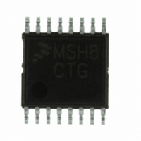
MC9S08SH8CTG Freescale Semiconductor, MC9S08SH8CTG Datasheet - Page 257

MC9S08SH8CTG
Manufacturer Part Number
MC9S08SH8CTG
Description
IC MCU 8BIT 8K FLASH 16-TSSOP
Manufacturer
Freescale Semiconductor
Series
HCS08r
Datasheet
1.MC9S08SH4CTJ.pdf
(338 pages)
Specifications of MC9S08SH8CTG
Core Processor
HCS08
Core Size
8-Bit
Speed
40MHz
Connectivity
I²C, LIN, SCI, SPI
Peripherals
LVD, POR, PWM, WDT
Number Of I /o
13
Program Memory Size
8KB (8K x 8)
Program Memory Type
FLASH
Ram Size
512 x 8
Voltage - Supply (vcc/vdd)
2.7 V ~ 5.5 V
Data Converters
A/D 8x10b
Oscillator Type
Internal
Operating Temperature
-40°C ~ 85°C
Package / Case
16-TSSOP
Cpu Family
HCS08
Device Core Size
8b
Frequency (max)
40MHz
Interface Type
I2C/SCI/SPI
Total Internal Ram Size
512Byte
# I/os (max)
13
Number Of Timers - General Purpose
1
Operating Supply Voltage (typ)
3.3/5V
Operating Supply Voltage (max)
5.5V
Operating Supply Voltage (min)
2.7V
On-chip Adc
8-chx10-bit
Instruction Set Architecture
CISC
Operating Temp Range
-40C to 85C
Operating Temperature Classification
Industrial
Mounting
Surface Mount
Pin Count
16
Package Type
TSSOP
Processor Series
S08SH
Core
HCS08
Data Bus Width
8 bit
Data Ram Size
512 B
Maximum Clock Frequency
40 MHz
Number Of Programmable I/os
13
Number Of Timers
3
Operating Supply Voltage
5.5 V
Maximum Operating Temperature
+ 85 C
Mounting Style
SMD/SMT
3rd Party Development Tools
EWS08
Development Tools By Supplier
DEMO9S08SG32, DEMO9S08SG32AUTO, DEMO9S08SG8, DEMO9S08SG8AUTO, DEMO9S08SH32, DEMO9S08SH8
Minimum Operating Temperature
- 40 C
For Use With
DEMO9S08SH8 - BOARD DEMO FOR MC9S08SH FAM
Lead Free Status / RoHS Status
Lead free / RoHS Compliant
Eeprom Size
-
Lead Free Status / Rohs Status
Compliant
Available stocks
Company
Part Number
Manufacturer
Quantity
Price
Company:
Part Number:
MC9S08SH8CTG
Manufacturer:
FREESCALE
Quantity:
12 000
Part Number:
MC9S08SH8CTG
Manufacturer:
FREESCALE
Quantity:
20 000
Part Number:
MC9S08SH8CTGR
Manufacturer:
FREESCALE
Quantity:
20 000
- Current page: 257 of 338
- Download datasheet (4Mb)
16.4.2.1
With the input-capture function, the TPM can capture the time at which an external event occurs. When an
active edge occurs on the pin of an input-capture channel, the TPM latches the contents of the TPM counter
into the channel-value registers (TPMxCnVH:TPMxCnVL). Rising edges, falling edges, or any edge may
be chosen as the active edge that triggers an input capture.
In input capture mode, the TPMxCnVH and TPMxCnVL registers are read only.
When either half of the 16-bit capture register is read, the other half is latched into a buffer to support
coherent 16-bit accesses in big-endian or little-endian order. The coherency sequence can be manually
reset by writing to the channel status/control register (TPMxCnSC).
An input capture event sets a flag bit (CHnF) which may optionally generate a CPU interrupt request.
While in BDM, the input capture function works as configured by the user. When an external event occurs,
the TPM latches the contents of the TPM counter (which is frozen because of the BDM mode) into the
channel value registers and sets the flag bit.
16.4.2.2
With the output-compare function, the TPM can generate timed pulses with programmable position,
polarity, duration, and frequency. When the counter reaches the value in the channel-value registers of an
output-compare channel, the TPM can set, clear, or toggle the channel pin.
In output compare mode, values are transferred to the corresponding timer channel registers only after both
8-bit halves of a 16-bit register have been written and according to the value of CLKSB:CLKSA bits, so:
The coherency sequence can be manually reset by writing to the channel status/control register
(TPMxCnSC).
An output compare event sets a flag bit (CHnF) which may optionally generate a CPU-interrupt request.
16.4.2.3
This type of PWM output uses the normal up-counting mode of the timer counter (CPWMS=0) and can
be used when other channels in the same TPM are configured for input capture or output compare
functions. The period of this PWM signal is determined by the value of the modulus register
(TPMxMODH:TPMxMODL) plus 1. The duty cycle is determined by the setting in the timer channel
register (TPMxCnVH:TPMxCnVL). The polarity of this PWM signal is determined by the setting in the
ELSnA control bit. 0% and 100% duty cycle cases are possible.
The output compare value in the TPM channel registers determines the pulse width (duty cycle) of the
PWM signal
width. If ELSnA=0, the counter overflow forces the PWM signal high, and the output compare forces the
PWM signal low. If ELSnA=1, the counter overflow forces the PWM signal low, and the output compare
forces the PWM signal high.
Freescale Semiconductor
•
•
If (CLKSB:CLKSA = 0:0), the registers are updated when the second byte is written
If (CLKSB:CLKSA not = 0:0), the registers are updated at the next change of the TPM counter
(end of the prescaler counting) after the second byte is written.
(Figure
Input Capture Mode
Output Compare Mode
Edge-Aligned PWM Mode
16-15). The time between the modulus overflow and the output compare is the pulse
MC9S08SH8 MCU Series Data Sheet, Rev. 3
Chapter 16 Timer/PWM Module (S08TPMV3)
257
Related parts for MC9S08SH8CTG
Image
Part Number
Description
Manufacturer
Datasheet
Request
R
Part Number:
Description:
Manufacturer:
Freescale Semiconductor, Inc
Datasheet:
Part Number:
Description:
Manufacturer:
Freescale Semiconductor, Inc
Datasheet:
Part Number:
Description:
Manufacturer:
Freescale Semiconductor, Inc
Datasheet:
Part Number:
Description:
Manufacturer:
Freescale Semiconductor, Inc
Datasheet:
Part Number:
Description:
Manufacturer:
Freescale Semiconductor, Inc
Datasheet:
Part Number:
Description:
Manufacturer:
Freescale Semiconductor, Inc
Datasheet:
Part Number:
Description:
Manufacturer:
Freescale Semiconductor, Inc
Datasheet:
Part Number:
Description:
Manufacturer:
Freescale Semiconductor, Inc
Datasheet:
Part Number:
Description:
Manufacturer:
Freescale Semiconductor, Inc
Datasheet:
Part Number:
Description:
Manufacturer:
Freescale Semiconductor, Inc
Datasheet:
Part Number:
Description:
Manufacturer:
Freescale Semiconductor, Inc
Datasheet:
Part Number:
Description:
Manufacturer:
Freescale Semiconductor, Inc
Datasheet:
Part Number:
Description:
Manufacturer:
Freescale Semiconductor, Inc
Datasheet:
Part Number:
Description:
Manufacturer:
Freescale Semiconductor, Inc
Datasheet:
Part Number:
Description:
Manufacturer:
Freescale Semiconductor, Inc
Datasheet:


