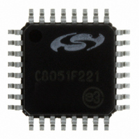
C8051F221-GQR Silicon Laboratories Inc, C8051F221-GQR Datasheet - Page 125

C8051F221-GQR
Manufacturer Part Number
C8051F221-GQR
Description
IC 8051 MCU 8K FLASH 32LQFP
Manufacturer
Silicon Laboratories Inc
Series
C8051F2xxr
Specifications of C8051F221-GQR
Core Processor
8051
Core Size
8-Bit
Speed
25MHz
Connectivity
SPI, UART/USART
Peripherals
Brown-out Detect/Reset, POR, WDT
Number Of I /o
22
Program Memory Size
8KB (8K x 8)
Program Memory Type
FLASH
Ram Size
256 x 8
Voltage - Supply (vcc/vdd)
2.7 V ~ 3.6 V
Data Converters
A/D 22x8b
Oscillator Type
Internal
Operating Temperature
-40°C ~ 85°C
Package / Case
32-LQFP
Processor Series
C8051F2x
Core
8051
Data Bus Width
8 bit
Data Ram Size
256 B
Interface Type
SPI, UART
Maximum Clock Frequency
25 MHz
Number Of Programmable I/os
32
Number Of Timers
3 bit
Operating Supply Voltage
2.7 V to 3.6 V
Maximum Operating Temperature
+ 85 C
Mounting Style
SMD/SMT
3rd Party Development Tools
PK51, CA51, A51, ULINK2
Development Tools By Supplier
C8051F226DK
Minimum Operating Temperature
- 40 C
On-chip Adc
8 bit, 32 Channel
For Use With
336-1241 - DEV KIT F220/221/226/230/231/236
Lead Free Status / RoHS Status
Lead free / RoHS Compliant
Eeprom Size
-
Lead Free Status / Rohs Status
Details
Available stocks
Company
Part Number
Manufacturer
Quantity
Price
Company:
Part Number:
C8051F221-GQR
Manufacturer:
Silicon Laboratories Inc
Quantity:
10 000
17. Timers
The CIP-51 implements three, 16-bit counter/timers comparable with those found in the standard 8051
MCU's. These can be used to measure time intervals, count external events and generate periodic inter-
rupt requests. Timer 0 and Timer 1 are nearly identical and have four primary modes of operation. Timer
2 offers additional capabilities not available in Timers 0 and 1, such as capture and baud rate generation.
When functioning as a timer, the counter/timer registers are incremented on each clock tick. Clock ticks
are derived from the system clock divided by either one or twelve as specified by the Timer Clock Select
bits (T2M–T0M) in CKCON. The twelve-clocks-per-tick option provides compatibility with the older gener-
ation of the 8051 family. Applications that require a faster timer can use the one-clock-per-tick option.
When functioning as a counter, a counter/timer register is incremented on each high-to-low transition at the
selected input pin (P0.4/T0, P0.5/T1, or P0.6/T2. Events with a frequency of up to one-fourth the system
clock's frequency can be counted. The input signal need not be periodic, but it should be held at a given
level for at least two full system clock cycles to ensure the level is sampled.
17.1. Timer 0 and Timer 1
Timer 0 and Timer 1 are accessed and controlled through SFR's. Each counter/timer is implemented as a
16-bit register accessed as two separate bytes: a low byte (TL0 or TL1) and a high byte (TH0 or TH1). The
Counter/Timer Control (TCON) register is used to enable Timer 0 and Timer 1 as well as indicate their sta-
tus. Both counter/timers operate in one of four primary modes selected by setting the Mode Select bits
M1–M0 in the Counter/Timer Mode (TMOD) register. Each timer can be configured independently. Follow-
ing is a detailed description of each operating mode.
17.1.1. Mode 0: 13-bit Counter/Timer
Timer 0 and Timer 1 operate as a 13-bit counter/timer in Mode 0. The following describes the configuration
and operation of Timer 0. However, both timers operate identically and Timer 1 is configured in the same
manner as described for Timer 0.
The TH0 register holds the eight MSB's of the 13-bit counter/timer. TL0 holds the five LSBs in bit positions
TL0.4–TL0.0. The three upper bits of TL0 (TL0.7–TL0.5) are indeterminate and should be masked out or
ignored when reading. As the 13-bit timer register increments and overflows from 0x1FFF (all ones) to
0x0000, the timer overflow flag TF0 (TCON.5) is set and an interrupt will occur if enabled.
The C/T0 bit (TMOD.2) selects the counter/timer's clock source. Clearing C/T selects the system clock as
the input for the timer. When C/T0 is set to logic 1, high-to-low transitions at the selected input pin incre-
ment the timer register. (Refer to section 14 for information on selecting and configuring external I/O pins.)
Setting the TR0 bit (TCON.4) enables the timer when either GATE0 (TMOD.3) is 0 or the input signal /INT0
is logic-level one. Setting GATE0 to logic 1 allows the timer to be controlled by the external input signal
/INT0, facilitating pulse width measurements.
13-bit counter/timer
16-bit counter/timer
8-bit counter/timer with auto-reload
Two 8-bit counter/timers (Timer 0 only)
Timer 0 and Timer 1:
Rev. 1.6
16-bit counter/timer with auto-reload
16-bit counter/timer with capture
Baud rate generator
Timer 2:
C8051F2xx
125


