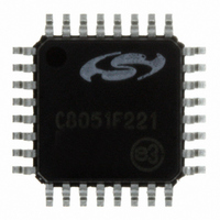
C8051F221-GQR Silicon Laboratories Inc, C8051F221-GQR Datasheet - Page 32

C8051F221-GQR
Manufacturer Part Number
C8051F221-GQR
Description
IC 8051 MCU 8K FLASH 32LQFP
Manufacturer
Silicon Laboratories Inc
Series
C8051F2xxr
Specifications of C8051F221-GQR
Core Processor
8051
Core Size
8-Bit
Speed
25MHz
Connectivity
SPI, UART/USART
Peripherals
Brown-out Detect/Reset, POR, WDT
Number Of I /o
22
Program Memory Size
8KB (8K x 8)
Program Memory Type
FLASH
Ram Size
256 x 8
Voltage - Supply (vcc/vdd)
2.7 V ~ 3.6 V
Data Converters
A/D 22x8b
Oscillator Type
Internal
Operating Temperature
-40°C ~ 85°C
Package / Case
32-LQFP
Processor Series
C8051F2x
Core
8051
Data Bus Width
8 bit
Data Ram Size
256 B
Interface Type
SPI, UART
Maximum Clock Frequency
25 MHz
Number Of Programmable I/os
32
Number Of Timers
3 bit
Operating Supply Voltage
2.7 V to 3.6 V
Maximum Operating Temperature
+ 85 C
Mounting Style
SMD/SMT
3rd Party Development Tools
PK51, CA51, A51, ULINK2
Development Tools By Supplier
C8051F226DK
Minimum Operating Temperature
- 40 C
On-chip Adc
8 bit, 32 Channel
For Use With
336-1241 - DEV KIT F220/221/226/230/231/236
Lead Free Status / RoHS Status
Lead free / RoHS Compliant
Eeprom Size
-
Lead Free Status / Rohs Status
Details
Available stocks
Company
Part Number
Manufacturer
Quantity
Price
Company:
Part Number:
C8051F221-GQR
Manufacturer:
Silicon Laboratories Inc
Quantity:
10 000
C8051F2xx
5.
Description
The ADC subsystem for the C8051F220/1/6 consists of configurable analog multiplexer (AMUX), a pro-
grammable gain amplifier (PGA), and a 100ksps, 8-bit successive-approximation-register ADC with inte-
grated track-and-hold and programmable window detector (see Figure 5.1). The AMUX, PGA, Data
Conversion Modes, and Window Detector are all configurable under software control via the Special Func-
tion Register's shown in Figure 5.1. The ADC subsystem (ADC, track-and-hold and PGA) is enabled only
when the ADCEN bit in the ADC Control register (ADC0CN, SFR Definition 5.3) is set to 1. The ADC sub-
system is in low power shutdown when this bit is 0.
5.1.
Any external port pin (ports 0-3) may be selected via software. The AMX0SL SFR is used to select the
desired analog input pin. (See SFR Definition 5.1). When the AMUX is enabled, the user selects which
port is to be used (bits PRTSL0-1), and then the pin in the selected port (bits PINSL0-2) to be the analog
input.
The table in
the AMUX output signal by an amount determined by the states of the AMPGN2-0 bits in the ADC Config-
uration register, ADC0CF (SFR Definition 5.2). The PGA can be software-programmed for gains of 0.5, 1,
2, 4, 8 or 16. It defaults to a gain of 1 on reset.
32
AIN31
AIN0
port pin may be configured as an
ADC (8-Bit, C8051F220/1/6 Only)
Analog Multiplexer and PGA
AIN0-31 are port 0-3
pins -- any external
analog input
??
shows AMUX functionality by channel for each possible configuration. The PGA amplifies
Figure 5.1. 8-Bit ADC Functional Block Diagram
32-to-1
AMUX
AMX0SL
X
GND
+
-
GND
VDD
ADCEN
ADC0GTH
ADC0CF
Rev. 1.6
ADC
VDD
8-Bit
SAR
ADC0CN
ADC0LTH
VDD
8
VREF
16
8
T2 OV
Comp
Dig
ADWINT


