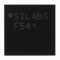
C8051F541-IM Silicon Laboratories Inc, C8051F541-IM Datasheet - Page 273

C8051F541-IM
Manufacturer Part Number
C8051F541-IM
Description
IC 8051 MCU 16K FLASH 32-QFN
Manufacturer
Silicon Laboratories Inc
Series
C8051F54xr
Specifications of C8051F541-IM
Program Memory Type
FLASH
Program Memory Size
16KB (16K x 8)
Package / Case
32-QFN
Mfg Application Notes
LIN Bootloader AppNote
Core Processor
8051
Core Size
8-Bit
Speed
50MHz
Connectivity
SMBus (2-Wire/I²C), SPI, UART/USART
Peripherals
POR, PWM, Temp Sensor, WDT
Number Of I /o
25
Ram Size
1.25K x 8
Voltage - Supply (vcc/vdd)
1.8 V ~ 5.25 V
Data Converters
A/D 25x12b
Oscillator Type
Internal
Operating Temperature
-40°C ~ 125°C
Processor Series
C8051F5x
Core
8051
Data Bus Width
8 bit
Data Ram Size
256 B
Maximum Clock Frequency
50 MHz
Number Of Programmable I/os
25
Operating Supply Voltage
1.8 V to 5.25 V
Maximum Operating Temperature
+ 125 C
Mounting Style
SMD/SMT
3rd Party Development Tools
PK51, CA51, A51, ULINK2
Development Tools By Supplier
C8051F540DK
Minimum Operating Temperature
- 40 C
Lead Free Status / RoHS Status
Lead free / RoHS Compliant
For Use With
336-1672 - BOARD PROTOTYPE W/C8051F540336-1669 - KIT DEVELOPMENT FOR C8051F540
Eeprom Size
-
Lead Free Status / Rohs Status
Lead free / RoHS Compliant
Other names
336-1673-5
- Current page: 273 of 274
- Download datasheet (3Mb)
D
Revision 0.1 to Revision 1.0
Note: All items from the C8051F54x Errata dated November 5th, 2009 are incorporated into this data sheet.
Revision 1.0 to Revision 1.1
OCUMENT
Updated “2. Ordering Information” to include -A (Automotive) devices and automotive qualification
information.
Updated Figure 4.6.
Updated supply current related specifications throughout “6. Electrical Characteristics” .
Updated SFR Definition 7.1 (REF0CN) to change VREF high setting to 2.20 V from 2.25 V.
Updated Figure 8.1 to indicate that Comparators are powered from V
Updated the Gain Table in “5.3.1. Calculating the Gain Value” to fix the ADC0GNH Value in the last row.
Updated Table 10.1 with correct timing for all branch instructions, MOVC, and CPL A.
Updated Table 14.1 to indicate behavior when performing a Flash operation in reserved space.
Updated “14.1. Programming the Flash Memory” to clarify behavior of 8-bit MOVX instructions and
when writing/erasing Flash.
Updated SFR Definition 14.3 (FLSCL) to include FLEWT bit definition. This bit must be set before
writing or erasing Flash. Also updated Table 6.5 to reflect new Flash Write and Erase timing.
Updated “16.7. Flash Error Reset” with an additional cause of a Flash Error reset.
Updated “18.1.3. Interfacing Port I/O in a Multi-Voltage System” to remove note regarding interfacing to
voltages above VIO.
Updated “20. SMBus” to remove all hardware ACK features, including SMB0ADM and SMB0ADR
SFRs.
Updated SFR Definition 21.1(SCON0) to correct SFR Page to 0x00 from All Pages.
Updated CP Register Definition 24.2 with proper Device ID.
Updated “1. System Overview” with a voltage range specification for the internal oscillator.
Updated Figure 5.4, “12-Bit ADC Burst Mode Example With Repeat Count Set to 4,” on page 33 with
new timing diagram when using CNVSTR pin.
Updated Table 6.6, “Internal High-Frequency Oscillator Electrical Characteristics,” on page 53 with new
conditions for the internal oscillator accuracy. The internal oscillator accuracy is dependent on the
operating voltage range.
Updated “6. Electrical Characteristics” to remove the internal oscillator curve across temperature
diagram.
Updated SFR Definition 7.1 (REF0CN) with oscillator suspend requirement for ZTCEN.
Fixed incorrect cross references in “8. Comparators” .
Updated SFR Definition 9.1 (REG0CN) with a new definition for Bit 6. The bit 6 reset value is 1b and
must be written to 1b.
Updated Figure 11.2, “Flash Program Memory Map,” on page 86 with correct address for start of lock
byte page from 0x3900 to 0x3A00.
Updated “15.3. Suspend Mode” with note regarding ZTCEN.
Added Port 2 Event and Port 3 Event to wake-up sources in “17.2.1. Internal Oscillator Suspend Mode”
Updated “19. Local Interconnect Network (LIN)” with a voltage range specification for the internal
oscillator.
Updated LIN Register Definitions for LIN0MUL and LIN0DIV to correct the reset value.
Updated C2 Register Definitions 25.2 and 25.3 with correct C2 and SFR addresses.
C
HANGE
L
IST
Rev. 1.1
IO
and not V
C8051F54x
DDA
.
273
Related parts for C8051F541-IM
Image
Part Number
Description
Manufacturer
Datasheet
Request
R
Part Number:
Description:
SMD/C°/SINGLE-ENDED OUTPUT SILICON OSCILLATOR
Manufacturer:
Silicon Laboratories Inc
Part Number:
Description:
Manufacturer:
Silicon Laboratories Inc
Datasheet:
Part Number:
Description:
N/A N/A/SI4010 AES KEYFOB DEMO WITH LCD RX
Manufacturer:
Silicon Laboratories Inc
Datasheet:
Part Number:
Description:
N/A N/A/SI4010 SIMPLIFIED KEY FOB DEMO WITH LED RX
Manufacturer:
Silicon Laboratories Inc
Datasheet:
Part Number:
Description:
N/A/-40 TO 85 OC/EZLINK MODULE; F930/4432 HIGH BAND (REV E/B1)
Manufacturer:
Silicon Laboratories Inc
Part Number:
Description:
EZLink Module; F930/4432 Low Band (rev e/B1)
Manufacturer:
Silicon Laboratories Inc
Part Number:
Description:
I°/4460 10 DBM RADIO TEST CARD 434 MHZ
Manufacturer:
Silicon Laboratories Inc
Part Number:
Description:
I°/4461 14 DBM RADIO TEST CARD 868 MHZ
Manufacturer:
Silicon Laboratories Inc
Part Number:
Description:
I°/4463 20 DBM RFSWITCH RADIO TEST CARD 460 MHZ
Manufacturer:
Silicon Laboratories Inc
Part Number:
Description:
I°/4463 20 DBM RADIO TEST CARD 868 MHZ
Manufacturer:
Silicon Laboratories Inc
Part Number:
Description:
I°/4463 27 DBM RADIO TEST CARD 868 MHZ
Manufacturer:
Silicon Laboratories Inc
Part Number:
Description:
I°/4463 SKYWORKS 30 DBM RADIO TEST CARD 915 MHZ
Manufacturer:
Silicon Laboratories Inc
Part Number:
Description:
N/A N/A/-40 TO 85 OC/4463 RFMD 30 DBM RADIO TEST CARD 915 MHZ
Manufacturer:
Silicon Laboratories Inc
Part Number:
Description:
I°/4463 20 DBM RADIO TEST CARD 169 MHZ
Manufacturer:
Silicon Laboratories Inc


