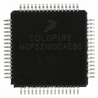
MCF52100CAE80 Freescale Semiconductor, MCF52100CAE80 Datasheet - Page 34

MCF52100CAE80
Manufacturer Part Number
MCF52100CAE80
Description
IC MCU 32BIT 80MHZ 64-LQFP
Manufacturer
Freescale Semiconductor
Series
MCF521xxr
Datasheet
1.MCF52110CAF80.pdf
(56 pages)
Specifications of MCF52100CAE80
Core Processor
Coldfire V2
Core Size
32-Bit
Speed
80MHz
Connectivity
I²C, SPI, UART/USART
Peripherals
DMA, LVD, POR, PWM, WDT
Number Of I /o
43
Program Memory Size
64KB (64K x 8)
Program Memory Type
FLASH
Ram Size
16K x 8
Voltage - Supply (vcc/vdd)
3 V ~ 3.6 V
Data Converters
A/D 8x12b
Oscillator Type
Internal
Operating Temperature
-40°C ~ 85°C
Package / Case
64-LQFP
Processor Series
MCF521x
Core
ColdFire V2
Data Bus Width
32 bit
Data Ram Size
16 KB
Interface Type
I2C/QSPI/UART
Maximum Clock Frequency
80 MHz
Number Of Programmable I/os
56
Number Of Timers
10
Operating Supply Voltage
- 0.3 V to + 4 V
Maximum Operating Temperature
+ 85 C
Mounting Style
SMD/SMT
3rd Party Development Tools
JLINK-CF-BDM26, EWCF
Development Tools By Supplier
M52210DEMO
Minimum Operating Temperature
- 40 C
On-chip Adc
8-ch x 12-bit
For Use With
M5211DEMO - KIT DEMO FOR MCF5211
Lead Free Status / RoHS Status
Lead free / RoHS Compliant
Eeprom Size
-
Lead Free Status / Rohs Status
Lead free / RoHS Compliant
2.10
2.11
Table 31
Freescale Semiconductor
1
2
NUM
All AC timing is shown with respect to 50% V
During low power STOP, the synchronizers for the RSTI input are bypassed and RSTI is asserted asynchronously to the
system. Thus, RSTI must be held a minimum of 100 ns.
R1
R2
R3
R4
lists specifications for the I
Reset Timing
RSTI input valid to CLKOUT High
CLKOUT High to RSTI Input invalid
RSTI input valid time
CLKOUT High to RSTO Valid
I
2
C Input/Output Timing Specifications
CLKOUT
RSTO
RSTI
GPIO Outputs
GPIO Inputs
Table 30. Reset and Configuration Override Timing
2
1R1
Figure 6. RSTI and Configuration Override Timing
CLKOUT
Characteristic
2
C input timing parameters shown in
(V
MCF52110 ColdFire Microcontroller, Rev. 1
DD
= 3.0 to 3.6 V, V
R3
Figure 5. GPIO Timing
DD
G3
levels unless otherwise noted.
SS
G1
R2
G4
= 0 V, T
R4
A
= T
Figure
Symbol
t
L
t
CHROV
G2
t
t
RVCH
CHRI
RIVT
to T
7.
H
)
1
Min
1.5
—
9
5
R4
Electrical Characteristics
Max
10
—
—
—
Unit
t
CYC
ns
ns
ns
34


