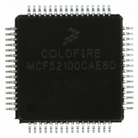
MCF52100CAE80 Freescale Semiconductor, MCF52100CAE80 Datasheet - Page 39

MCF52100CAE80
Manufacturer Part Number
MCF52100CAE80
Description
IC MCU 32BIT 80MHZ 64-LQFP
Manufacturer
Freescale Semiconductor
Series
MCF521xxr
Datasheet
1.MCF52110CAF80.pdf
(56 pages)
Specifications of MCF52100CAE80
Core Processor
Coldfire V2
Core Size
32-Bit
Speed
80MHz
Connectivity
I²C, SPI, UART/USART
Peripherals
DMA, LVD, POR, PWM, WDT
Number Of I /o
43
Program Memory Size
64KB (64K x 8)
Program Memory Type
FLASH
Ram Size
16K x 8
Voltage - Supply (vcc/vdd)
3 V ~ 3.6 V
Data Converters
A/D 8x12b
Oscillator Type
Internal
Operating Temperature
-40°C ~ 85°C
Package / Case
64-LQFP
Processor Series
MCF521x
Core
ColdFire V2
Data Bus Width
32 bit
Data Ram Size
16 KB
Interface Type
I2C/QSPI/UART
Maximum Clock Frequency
80 MHz
Number Of Programmable I/os
56
Number Of Timers
10
Operating Supply Voltage
- 0.3 V to + 4 V
Maximum Operating Temperature
+ 85 C
Mounting Style
SMD/SMT
3rd Party Development Tools
JLINK-CF-BDM26, EWCF
Development Tools By Supplier
M52210DEMO
Minimum Operating Temperature
- 40 C
On-chip Adc
8-ch x 12-bit
For Use With
M5211DEMO - KIT DEMO FOR MCF5211
Lead Free Status / RoHS Status
Lead free / RoHS Compliant
Eeprom Size
-
Lead Free Status / Rohs Status
Lead free / RoHS Compliant
Electrical Characteristics
39
1
J1
J2
J3
J4
J5
J6
J7
J8
J9
J10
J11
J12
J13
J14
Num
JTAG_EN is expected to be a static signal. Hence, it is not associated with any timing.
TCLK
(input)
TCLK frequency of operation
TCLK cycle period
TCLK clock pulse width
TCLK rise and fall times
Boundary scan input data setup time to TCLK rise
Boundary scan input data hold time after TCLK rise
TCLK low to boundary scan output data valid
TCLK low to boundary scan output high Z
TMS, TDI input data setup time to TCLK rise
TMS, TDI Input data hold time after TCLK rise
TCLK low to TDO data valid
TCLK low to TDO high Z
TRST assert time
TRST setup time (negation) to TCLK high
Characteristics
Table 36. JTAG and Boundary Scan Timing
J4
V
MCF52110 ColdFire Microcontroller, Rev. 1
IH
Figure 10. Test Clock Input Timing
V
IL
1
J3
J4
J2
Symbol
t
t
t
t
t
t
t
t
TAPBST
TAPBHT
TRSTST
TRSTAT
TDODZ
f
t
BSDST
BSDHT
t
t
TDODV
t
t
JCYC
JCYC
BSDV
BSDZ
JCRF
JCW
J3
4 t
Min
100
DC
26
26
10
10
0
4
0
0
4
0
0
CYC
Freescale Semiconductor
Max
1/4
33
33
26
—
—
—
—
—
—
—
—
3
8
f
Unit
sys/2
ns
ns
ns
ns
ns
ns
ns
ns
ns
ns
ns
ns
ns


