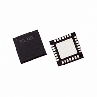
C8051F311-GMR Silicon Laboratories Inc, C8051F311-GMR Datasheet - Page 180

C8051F311-GMR
Manufacturer Part Number
C8051F311-GMR
Description
IC 8051 MCU 16K FLASH 28MLP
Manufacturer
Silicon Laboratories Inc
Series
C8051F31xr
Specifications of C8051F311-GMR
Core Processor
8051
Core Size
8-Bit
Speed
25MHz
Connectivity
SMBus (2-Wire/I²C), SPI, UART/USART
Peripherals
POR, PWM, Temp Sensor, WDT
Number Of I /o
25
Program Memory Size
16KB (16K x 8)
Program Memory Type
FLASH
Ram Size
1.25K x 8
Voltage - Supply (vcc/vdd)
2.7 V ~ 3.6 V
Data Converters
A/D 17x10b
Oscillator Type
Internal
Operating Temperature
-40°C ~ 85°C
Package / Case
28-VQFN Exposed Pad, 28-HVQFN, 28-SQFN, 28-DHVQFN
Package
24QFN EP
Device Core
8051
Family Name
C8051F31x
Maximum Speed
25 MHz
Operating Supply Voltage
3.3 V
Data Bus Width
8 Bit
Number Of Programmable I/os
25
Interface Type
I2C/SMBus/SPI/UART
On-chip Adc
17-chx10-bit
Number Of Timers
4
For Use With
336-1446 - ADAPTER PROGRAM TOOLSTICK F311336-1253 - DEV KIT FOR C8051F310/F311
Lead Free Status / RoHS Status
Lead free / RoHS Compliant
Eeprom Size
-
Available stocks
Company
Part Number
Manufacturer
Quantity
Price
Part Number:
C8051F311-GMR
Manufacturer:
SILICON LABS/芯科
Quantity:
20 000
C8051F310/1/2/3/4/5/6/7
16.6. SPI Special Function Registers
SPI0 is accessed and controlled through four special function registers in the system controller: SPI0CN
Control Register, SPI0DAT Data Register, SPI0CFG Configuration Register, and SPI0CKR Clock Rate
Register. The four special function registers related to the operation of the SPI0 Bus are described in the
following register definitions.
180
Bit 7:
Bit 6:
Bit 5:
Bit 4:
Bit 3:
Bit 2:
Bit 1:
Bit 0:
*Note:
SPIBSY
Bit7
R
SPIBSY: SPI Busy (read only).
This bit is set to logic 1 when a SPI transfer is in progress (Master or slave Mode).
MSTEN: Master Mode Enable.
0: Disable master mode. Operate in slave mode.
1: Enable master mode. Operate as a master.
CKPHA: SPI0 Clock Phase.
This bit controls the SPI0 clock phase.
0: Data centered on first edge of SCK period.*
1: Data centered on second edge of SCK period.*
CKPOL: SPI0 Clock Polarity.
This bit controls the SPI0 clock polarity.
0: SCK line low in idle state.
1: SCK line high in idle state.
SLVSEL: Slave Selected Flag (read only).
This bit is set to logic 1 whenever the NSS pin is low indicating SPI0 is the selected slave. It
is cleared to logic 0 when NSS is high (slave not selected). This bit does not indicate the
instantaneous value at the NSS pin, but rather a de-glitched version of the pin input.
NSSIN: NSS Instantaneous Pin Input (read only).
This bit mimics the instantaneous value that is present on the NSS port pin at the time that
the register is read. This input is not de-glitched.
SRMT: Shift Register Empty (Valid in Slave Mode, read only).
This bit will be set to logic 1 when all data has been transferred in/out of the shift register,
and there is no new information available to read from the transmit buffer or write to the
receive buffer. It returns to logic 0 when a data byte is transferred to the shift register from
the transmit buffer or by a transition on SCK.
NOTE: SRMT = 1 when in Master Mode.
RXBMT: Receive Buffer Empty (Valid in Slave Mode, read only).
This bit will be set to logic 1 when the receive buffer has been read and contains no new
information. If there is new information available in the receive buffer that has not been read,
this bit will return to logic 0.
NOTE: RXBMT = 1 when in Master Mode.
sampled one SYSCLK before the end of each data bit, to provide maximum settling time for the slave
device. See Table 16.1 for timing parameters.
In slave mode, data on MOSI is sampled in the center of each data bit. In master mode, data on MISO is
MSTEN
R/W
Bit6
SFR Definition 16.1. SPI0CFG: SPI0 Configuration
CKPHA
R/W
Bit5
CKPOL
R/W
Bit4
SLVSEL
Rev. 1.7
Bit3
R
NSSIN
Bit2
R
SRMT
Bit1
R
SFR Address: 0xA1
RXBMT
Bit0
R
Reset Value
00000111


