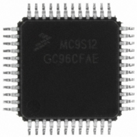
MC9S12GC16CFAE Freescale Semiconductor, MC9S12GC16CFAE Datasheet - Page 124

MC9S12GC16CFAE
Manufacturer Part Number
MC9S12GC16CFAE
Description
IC MCU 16K FLASH 25MHZ 48-LQFP
Manufacturer
Freescale Semiconductor
Series
HCS12r
Datasheet
1.MC9S12GC16MFUE.pdf
(690 pages)
Specifications of MC9S12GC16CFAE
Core Processor
HCS12
Core Size
16-Bit
Speed
25MHz
Connectivity
EBI/EMI, SCI, SPI
Peripherals
POR, PWM, WDT
Number Of I /o
31
Program Memory Size
16KB (16K x 8)
Program Memory Type
FLASH
Ram Size
1K x 8
Voltage - Supply (vcc/vdd)
2.35 V ~ 5.5 V
Data Converters
A/D 8x10b
Oscillator Type
Internal
Operating Temperature
-40°C ~ 85°C
Package / Case
48-LQFP
Processor Series
S12GC
Core
HCS12
Data Bus Width
16 bit
Data Ram Size
1 KB
Interface Type
CAN, SCI, SPI
Maximum Clock Frequency
25 MHz
Number Of Programmable I/os
31
Number Of Timers
8
Maximum Operating Temperature
+ 85 C
Mounting Style
SMD/SMT
3rd Party Development Tools
EWHCS12
Development Tools By Supplier
M68EVB912C32EE, M68DKIT912C32SLK
Minimum Operating Temperature
- 40 C
On-chip Adc
10 bit, 8 Channel
Package
48LQFP
Family Name
HCS12
Maximum Speed
25 MHz
Operating Supply Voltage
2.5|5 V
Lead Free Status / RoHS Status
Lead free / RoHS Compliant
Eeprom Size
-
Lead Free Status / Rohs Status
Details
Available stocks
Company
Part Number
Manufacturer
Quantity
Price
Company:
Part Number:
MC9S12GC16CFAE
Manufacturer:
Freescale Semiconductor
Quantity:
135
Company:
Part Number:
MC9S12GC16CFAE
Manufacturer:
Freescale Semiconductor
Quantity:
10 000
- Current page: 124 of 690
- Download datasheet (4Mb)
Chapter 3 Module Mapping Control (MMCV4) Block Description
unimplemented locations within the register space or to locations that are removed from the map (i.e., ports
A and B in expanded modes) will not cause this signal to become active. When the EMK bit is clear, this
pin is used for general purpose I/O.
3.4.3
The HCS12 core architecture limits the physical address space available to 64K bytes. The program page
index register allows for integrating up to 1M byte of FLASH or ROM into the system by using the six
page index bits to page 16K byte blocks into the program page window located from 0x8000 to 0xBFFF
in the physical memory space. The paged memory space can consist of solely on-chip memory or a
combination of on-chip and off-chip memory. This partitioning is configured at system integration through
the use of the paging configuration switches (pag_sw1:pag_sw0) at the core boundary. The options
available to the integrator are as given in
easy reference).
Based upon the system configuration, the program page window will consider its access to be either
internal or external as defined in
124
Memory Expansion
The partitioning as defined in
memory space and the actual on-chip memory sizes implemented in the
system may differ. Please refer to the device overview chapter for actual
sizes.
pag_sw1:pag_sw0
pag_sw1:pag_sw0
00
01
10
11
00
01
10
11
Table 3-17. External/Internal Page Window Access
Table 3-16. Allocated Off-Chip Memory Options
Table
MC9S12C-Family / MC9S12GC-Family
876K off-Chip,
128K on-Chip
768K off-chip,
512K off-chip,
256K on-chip
512K on-chip
Partitioning
0K off-chip,
1M on-chip
3-17.
Table 3-16
Table 3-17
Off-Chip Space
876K bytes
768K bytes
512K bytes
Rev 01.24
NOTE
0K byte
(this table matches
0x0038–0x003F
0x0000–0x002F
0x0030–0x003F
0x0000–0x001F
0x0020–0x003F
0x0000–0x003F
0x0000–0x0037
PIX5:0 Value
applies only to the allocated
N/A
Table 3-12
On-Chip Space
Page Window
128K bytes
256K bytes
512K bytes
External
External
External
External
1M byte
Access
Internal
Internal
Internal
Internal
but is repeated here for
Freescale Semiconductor
Related parts for MC9S12GC16CFAE
Image
Part Number
Description
Manufacturer
Datasheet
Request
R
Part Number:
Description:
Manufacturer:
Freescale Semiconductor, Inc
Datasheet:
Part Number:
Description:
Manufacturer:
Freescale Semiconductor, Inc
Datasheet:
Part Number:
Description:
Manufacturer:
Freescale Semiconductor, Inc
Datasheet:
Part Number:
Description:
Manufacturer:
Freescale Semiconductor, Inc
Datasheet:
Part Number:
Description:
Manufacturer:
Freescale Semiconductor, Inc
Datasheet:
Part Number:
Description:
Manufacturer:
Freescale Semiconductor, Inc
Datasheet:
Part Number:
Description:
Manufacturer:
Freescale Semiconductor, Inc
Datasheet:
Part Number:
Description:
Manufacturer:
Freescale Semiconductor, Inc
Datasheet:
Part Number:
Description:
Manufacturer:
Freescale Semiconductor, Inc
Datasheet:
Part Number:
Description:
Manufacturer:
Freescale Semiconductor, Inc
Datasheet:
Part Number:
Description:
Manufacturer:
Freescale Semiconductor, Inc
Datasheet:
Part Number:
Description:
Manufacturer:
Freescale Semiconductor, Inc
Datasheet:
Part Number:
Description:
Manufacturer:
Freescale Semiconductor, Inc
Datasheet:
Part Number:
Description:
Manufacturer:
Freescale Semiconductor, Inc
Datasheet:
Part Number:
Description:
Manufacturer:
Freescale Semiconductor, Inc
Datasheet:


