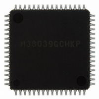
M38039GCHKP#U0 Renesas Electronics America, M38039GCHKP#U0 Datasheet - Page 88

M38039GCHKP#U0
Manufacturer Part Number
M38039GCHKP#U0
Description
IC 740/3803 MCU QZROM 64LQFP
Manufacturer
Renesas Electronics America
Series
740/38000r
Datasheet
1.M38039G4HHPU0.pdf
(105 pages)
Specifications of M38039GCHKP#U0
Core Processor
740
Core Size
8-Bit
Speed
16.8MHz
Connectivity
SIO, UART/USART
Peripherals
LED, PWM, WDT
Number Of I /o
56
Program Memory Size
48KB (48K x 8)
Program Memory Type
QzROM
Ram Size
2K x 8
Voltage - Supply (vcc/vdd)
1.8 V ~ 5.5 V
Data Converters
A/D 16x10b; D/A 2x8b
Oscillator Type
Internal
Operating Temperature
-20°C ~ 85°C
Package / Case
64-LQFP
Lead Free Status / RoHS Status
Lead free / RoHS Compliant
Eeprom Size
-
Available stocks
Company
Part Number
Manufacturer
Quantity
Price
3803 Group (Spec.H QzROM version)
REJ03B0166-0113 Rev.1.13
Page 86 of 100
Notes on Using Stop Mode
• Register setting
Since values of the prescaler 12 and Timer 1 are automatically
reloaded when returning from the stop mode, set them again,
respectively. (When the oscillation stabilizing time set after STP
instruction released bit is “0”)
• Clock restoration
After restoration from the stop mode to the normal mode by an
interrupt request, the contents of the CPU mode register previous
to the STP instruction execution are retained. Accordingly, if
both main clock and sub clock were oscillating before execution
of the STP instruction, the oscillation of both clocks is resumed
at restoration.
In the above case, when the main clock side is set as a system
clock, the oscillation stabilizing time for approximately 8,000
cycles of the X
mode. At this time, note that the oscillation on the sub clock side
may not be stabilized even after the lapse of the oscillation
stabilizing time of the main clock side.
Notes on Wait Mode
• Clock restoration
If the wait mode is released by a reset when X
system clock and X
the WIT instruction, X
starts, and X
In the above case, the RESET pin should be held at “L” until the
oscillation is stabilized.
Notes on Handling of Power Source Pins
In order to avoid a latch-up occurrence, connect a capacitor
suitable for high frequencies as bypass capacitor between power
source pin (V
source pin (V
pin). Besides, connect the capacitor to as close as possible. For
bypass capacitor which should not be located too far from the
pins to be connected, a ceramic capacitor of 0.01
recommended.
Notes on Power Source Voltage
When the power source voltage value of a microcomputer is less
than the value which is indicated as the recommended operating
conditions, the microcomputer does not operate normally and
may perform unstable operation.
In a system where the power source voltage drops slowly when
the power source voltage drops or the power supply is turned off,
reset a microcomputer when the power source voltage is less
than the recommended operating conditions and design a system
not to cause errors to the system by this unstable operation.
IN
CC
CC
is set as the system clock.
IN
pin) and GND pin (V
pin) and analog power source input pin (AV
input is reserved at restoration from the stop
IN
oscillation is stopped during execution of
CIN
oscillation stops, X
SS
Aug 21, 2009
pin), and between power
CIN
IN
µ
oscillations
is set as the
F–0.1
µ
F is
SS
Notes on Product Shipped in Blank
As for the product shipped in blank, Renesas does not perform
the writing test to user ROM area after the assembly process
though the QzROM writing test is performed enough before the
assembly process. Therefore, a writing error of approx.0.1 %
may occur. Moreover, please note the contact of cables and
foreign bodies on a socket, etc. because a writing environment
may cause some writing errors.
Precautions Regarding Overvoltage in QzROM Version
Make sure that voltage exceeding the V
applied to other pins. In particular, ensure that the state indicated
by bold lines in figure below does not occur for CNV
power source pin for QzROM) during power-on or power-off.
Otherwise the contents of QzROM could be rewritten.
Fig 84. Timing Diagram (bold-lined periods are applicable)
Notes on QzROM Version
Connect the CNV
pattern which is supplied to the V
In addition connecting an approximately 5 kΩ resistor in series to
the GND could improve noise immunity. In this case as well as
the above mention, connect the pin the shortest possible to the
GND pattern which is supplied to the V
microcomputer.
• Reason
The CNV
QzROM. When programming in the QzROM, the impedance of
the V
into the built-in QzROM. Because of this, noise can enter easily.
If noise enters the V
are read from the QzROM, which may cause a program runaway.
Fig 85. Wiring for the CNV
CNV
V
CC
pin voltage
SS
PP
pin voltage
pin is low to allow the electric current for writing to flow
(1) The input voltage to other MCU pins rises before the V
(2) The input voltage to other MCU pins falls before the V
Note: If V
SS
Note. Shows the microcomputer’s pin.
voltage rises.
voltage falls.
/V
the internal circuit becomes unstable. Take additional care
to prevent overvoltage.
PP
CNV
CC
pin is the power source input pin for the built-in
SS
1.8 V
falls below the minimum value 1.8 V (shaded areas),
SS
/V
PP
/V
PP
V
pin, abnormal instruction codes or data
PP
SS
pin the shortest possible to the GND
(1)
(Note)
(Note)
SS
/V
SS
PP
pin of the microcomputer.
Approx. 5kΩ
The shortest
The shortest
CC
pin voltage is not
S S
(2)
pin of the
SS
CC
CC
1.8 V
pin
pin (V
pin
PP


