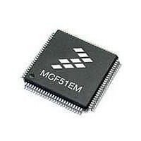
MCF51EM128CLL Freescale Semiconductor, MCF51EM128CLL Datasheet - Page 86

MCF51EM128CLL
Manufacturer Part Number
MCF51EM128CLL
Description
IC MCU 32BIT 128KB FLASH 100LQFP
Manufacturer
Freescale Semiconductor
Series
MCF51EMr
Datasheets
1.MCF51EM128CLL.pdf
(2 pages)
2.MCF51EM128CLL.pdf
(54 pages)
3.MCF51EM128CLL.pdf
(636 pages)
Specifications of MCF51EM128CLL
Core Processor
Coldfire V1
Core Size
32-Bit
Speed
50MHz
Connectivity
I²C, SCI, SPI
Peripherals
LCD, LVD, PWM, WDT
Number Of I /o
63
Program Memory Size
128KB (128K x 8)
Program Memory Type
FLASH
Ram Size
8K x 8
Voltage - Supply (vcc/vdd)
1.8 V ~ 3.6 V
Data Converters
A/D 16x12b
Oscillator Type
External
Operating Temperature
-40°C ~ 85°C
Package / Case
100-LQFP
Processor Series
MCF51EM
Core
ColdFire V1
Data Bus Width
32 bit
Data Ram Size
16 KB
Interface Type
RS-232, LIN
Maximum Clock Frequency
50 MHz
Number Of Timers
3
Operating Supply Voltage
1.8 V to 3.6 V
Maximum Operating Temperature
+ 85 C
Mounting Style
SMD/SMT
3rd Party Development Tools
JLINK-CF-BDM26, EWCF
Development Tools By Supplier
TWR-MCF51CN-KIT, TWR-SER, TWR-ELEV, TOWER
Minimum Operating Temperature
- 40 C
Lead Free Status / RoHS Status
Lead free / RoHS Compliant
Eeprom Size
-
Lead Free Status / Rohs Status
Lead free / RoHS Compliant
Available stocks
Company
Part Number
Manufacturer
Quantity
Price
Company:
Part Number:
MCF51EM128CLL
Manufacturer:
Freescale Semiconductor
Quantity:
10 000
- Current page: 86 of 636
- Download datasheet (11Mb)
Memory
Note that swapping flash arrays as discussed above does NOT change the location of the flash controllers
in the memory map. Registers in FTSR1 and FTSR2 are fixed in the memory map. Only the flash arrays
are impacted by changing IRTC_CFG_DATA[CFG0].
3.4.3
The flash controller (AKA FTSR) contains a set of 16 control and status registers. Detailed descriptions
of each register bit are provided in the following sections.
3.4.3.1
The FxCDIV register controls the length of timed events in program and erase algorithms executed by the
flash memory controller. All bits in the FxCDIV register are readable and writable with restrictions as
determined by the value of FDIVLD when writing to the FxCDIV register.
3-30
FDIVLD
PRDIV8
Reset
Field
FDIV
5–0
7
6
W
R
FDIVLD
Register Descriptions
Clock Divider Load Control. When writing to the FxCDIV register for the first time after a reset, the value of the
FDIVLD bit written controls the future ability to write to the FxCDIV register:
0 Writing a 0 to FDIVLD locks the FxCDIV register contents; all future writes to FxCDIV are ignored.
1 Writing a 1 to FDIVLD keeps the FxCDIV register writable; next write to FxCDIV is allowed.
When reading the FxCDIV register, the value of the FDIVLD bit read indicates the following:
0 FxCDIV register has not been written to since the last reset.
1 FxCDIV register has been written to since the last reset.
Enable Prescalar by 8
0 The bus clock is directly fed into the clock divider
1 The bus clock is divided by 8 before feeding into the clock divider.
Clock Divider Bits. The combination of PRDIV8 and FDIV[5:0] must divide the bus clock down to a frequency
of 150 kHz–200 kHz. The minimum divide ratio is 2 (PRDIV8 = 0, FDIV = 0x01) and the maximum divide ratio is
512 (PRDIV8 = 1, FDIV = 0x3F).
Flash Clock Divider Register (FxCDIV)
0
7
MCF51EM256 Series ColdFire Integrated Microcontroller Reference Manual, Rev. 8
IRTC_CFG_DATA[CFG0]
PRDIV8
0 (initial POR value)
0
6
Figure 3-3. Flash Clock Divider Register (FxCDIV)
.
1
Table 3-7. FxCDIV Field Descriptions
Table 3-6. Flash Array Base Address
0
5
FTSR1
FTSR2
FTSR1
FTSR2
Array
0
4
Description
.
0x(00)00_0000
0x(00)02_0000
0x(00)00_0000
MCF51EM256
3
0
FDIV
0x(00)00_0000
0x(00)01_0000
0x(00)00_0000
MCF51EM128
0
2
Freescale Semiconductor
0
1
0
0
Related parts for MCF51EM128CLL
Image
Part Number
Description
Manufacturer
Datasheet
Request
R

Part Number:
Description:
IC MCU 32BIT 256KB FLASH 100LQFP
Manufacturer:
Freescale Semiconductor
Datasheet:

Part Number:
Description:
BOARD DEMO HARDWARE ONLY
Manufacturer:
Freescale Semiconductor
Datasheet:

Part Number:
Description:
IC MCU 32BIT 128KB FLASH 80LQFP
Manufacturer:
Freescale Semiconductor
Datasheet:

Part Number:
Description:
IC MCU 32BIT 256KB FLASH 80LQFP
Manufacturer:
Freescale Semiconductor
Datasheet:
Part Number:
Description:
Manufacturer:
Freescale Semiconductor, Inc
Datasheet:
Part Number:
Description:
Manufacturer:
Freescale Semiconductor, Inc
Datasheet:
Part Number:
Description:
Manufacturer:
Freescale Semiconductor, Inc
Datasheet:
Part Number:
Description:
Manufacturer:
Freescale Semiconductor, Inc
Datasheet:
Part Number:
Description:
Manufacturer:
Freescale Semiconductor, Inc
Datasheet:
Part Number:
Description:
Manufacturer:
Freescale Semiconductor, Inc
Datasheet:
Part Number:
Description:
Manufacturer:
Freescale Semiconductor, Inc
Datasheet:
Part Number:
Description:
Manufacturer:
Freescale Semiconductor, Inc
Datasheet:
Part Number:
Description:
Manufacturer:
Freescale Semiconductor, Inc
Datasheet:
Part Number:
Description:
Manufacturer:
Freescale Semiconductor, Inc
Datasheet:


