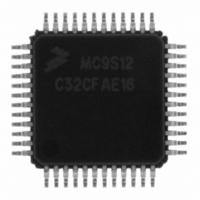
MC9S12C32CFAE16 Freescale Semiconductor, MC9S12C32CFAE16 Datasheet - Page 676

MC9S12C32CFAE16
Manufacturer Part Number
MC9S12C32CFAE16
Description
IC MCU 32K FLASH 16MHZ 48-LQFP
Manufacturer
Freescale Semiconductor
Series
HCS12r
Datasheets
1.MC9S12GC16MFUE.pdf
(690 pages)
2.MC9S12C96CFUER.pdf
(26 pages)
3.MC9S12C32CFAE25.pdf
(2 pages)
Specifications of MC9S12C32CFAE16
Core Processor
HCS12
Core Size
16-Bit
Speed
16MHz
Connectivity
CAN, EBI/EMI, SCI, SPI
Peripherals
POR, PWM, WDT
Number Of I /o
31
Program Memory Size
32KB (32K x 8)
Program Memory Type
FLASH
Ram Size
2K x 8
Voltage - Supply (vcc/vdd)
2.35 V ~ 5.5 V
Data Converters
A/D 8x10b
Oscillator Type
Internal
Operating Temperature
-40°C ~ 85°C
Package / Case
48-LQFP
Cpu Family
HCS12
Device Core Size
16b
Frequency (max)
16MHz
Interface Type
CAN/SCI/SPI
Total Internal Ram Size
2KB
# I/os (max)
31
Number Of Timers - General Purpose
8
Operating Supply Voltage (typ)
2.5/5V
Operating Supply Voltage (max)
2.75/5.5V
Operating Supply Voltage (min)
2.35/2.97V
On-chip Adc
8-chx10-bit
Instruction Set Architecture
CISC
Operating Temp Range
-40C to 85C
Operating Temperature Classification
Industrial
Mounting
Surface Mount
Pin Count
48
Package Type
LQFP
Package
48LQFP
Family Name
HCS12
Maximum Speed
16 MHz
Operating Supply Voltage
2.5|5 V
Data Bus Width
16 Bit
Number Of Programmable I/os
31
Number Of Timers
8
For Use With
CML12C32SLK - KIT STUDENT LEARNING 16BIT HCS12
Lead Free Status / RoHS Status
Lead free / RoHS Compliant
Eeprom Size
-
Lead Free Status / Rohs Status
Compliant
Available stocks
Company
Part Number
Manufacturer
Quantity
Price
Company:
Part Number:
MC9S12C32CFAE16
Manufacturer:
Freescale Semiconductor
Quantity:
10 000
- Current page: 676 of 690
- Download datasheet (4Mb)
Appendix A Electrical Characteristics
In
In
1. t
676
Num
10
11
12
13
bus
Figure A-9
Table A-22
1
1
2
3
4
5
6
7
8
9
(CPOL = 0)
(CPOL = 1)
(OUTPUT)
added due to internal synchronization delay
(INPUT)
NOTE: Not defined!
(INPUT)
(INPUT)
(INPUT)
MISO
MOSI
SCK
SCK
SS
C
D
P
D
D
D
D
D
D
D
D
D
D
D
D
the timing diagram for slave mode with transmission format CPHA=1 is depicted.
the timing characteristics for slave mode are listed.
SCK Frequency
SCK Period
Enable Lead Time
Enable Lag Time
Clock (SCK) High or Low Time
Data Setup Time (Inputs)
Data Hold Time (Inputs)
Slave Access Time (time to data active)
Slave MISO Disable Time
Data Valid after SCK Edge
Data Valid after SS fall
Data Hold Time (Outputs)
Rise and Fall Time Inputs
Rise and Fall Time Outputs
note
see
7
2
SLAVE
4
5
Table A-22. SPI Slave Mode Timing Characteristics
9
MSB IN
Characteristic
1
Figure A-9. SPI Slave Timing (CPHA=1)
MSB OUT
6
4
MC9S12C-Family / MC9S12GC-Family
12
12
11
BIT 6 . . . 1
BIT 6 . . . 1
Rev 01.24
Symbol
t
t
t
f
t
wsck
t
t
t
vsck
lead
t
t
t
sck
sck
t
vss
t
lag
t
dis
ho
rfo
su
hi
rfi
a
13
13
SLAVE LSB OUT
3
Min
DC
20
LSB IN
—
—
—
—
—
—
4
4
4
4
8
8
Typ
—
—
—
—
—
—
—
—
—
—
—
—
—
—
8
Freescale Semiconductor
30 + t
30 + t
Max
1/4
—
—
—
—
—
20
22
—
(1)
∞
8
8
bus
bus
1
Unit
f
t
t
t
t
ns
ns
ns
ns
ns
ns
ns
bus
bus
bus
bus
bus
ns
ns
Related parts for MC9S12C32CFAE16
Image
Part Number
Description
Manufacturer
Datasheet
Request
R
Part Number:
Description:
Manufacturer:
Freescale Semiconductor, Inc
Datasheet:
Part Number:
Description:
Manufacturer:
Freescale Semiconductor, Inc
Datasheet:
Part Number:
Description:
Manufacturer:
Freescale Semiconductor, Inc
Datasheet:
Part Number:
Description:
Manufacturer:
Freescale Semiconductor, Inc
Datasheet:
Part Number:
Description:
Manufacturer:
Freescale Semiconductor, Inc
Datasheet:
Part Number:
Description:
Manufacturer:
Freescale Semiconductor, Inc
Datasheet:
Part Number:
Description:
Manufacturer:
Freescale Semiconductor, Inc
Datasheet:
Part Number:
Description:
Manufacturer:
Freescale Semiconductor, Inc
Datasheet:
Part Number:
Description:
Manufacturer:
Freescale Semiconductor, Inc
Datasheet:
Part Number:
Description:
Manufacturer:
Freescale Semiconductor, Inc
Datasheet:
Part Number:
Description:
Manufacturer:
Freescale Semiconductor, Inc
Datasheet:
Part Number:
Description:
Manufacturer:
Freescale Semiconductor, Inc
Datasheet:
Part Number:
Description:
Manufacturer:
Freescale Semiconductor, Inc
Datasheet:
Part Number:
Description:
Manufacturer:
Freescale Semiconductor, Inc
Datasheet:
Part Number:
Description:
Manufacturer:
Freescale Semiconductor, Inc
Datasheet:


