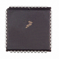
MC68HC711D3CFNE3 Freescale Semiconductor, MC68HC711D3CFNE3 Datasheet - Page 62

MC68HC711D3CFNE3
Manufacturer Part Number
MC68HC711D3CFNE3
Description
IC MCU 8BIT 2MHZ 44-PLCC
Manufacturer
Freescale Semiconductor
Series
HC11r
Specifications of MC68HC711D3CFNE3
Core Processor
HC11
Core Size
8-Bit
Speed
3MHz
Connectivity
SCI, SPI
Peripherals
POR, WDT
Number Of I /o
26
Program Memory Size
4KB (4K x 8)
Program Memory Type
OTP
Ram Size
192 x 8
Voltage - Supply (vcc/vdd)
4.5 V ~ 5.5 V
Oscillator Type
Internal
Operating Temperature
-40°C ~ 85°C
Package / Case
44-PLCC
Lead Free Status / RoHS Status
Lead free / RoHS Compliant
Eeprom Size
-
Data Converters
-
Available stocks
Company
Part Number
Manufacturer
Quantity
Price
Company:
Part Number:
MC68HC711D3CFNE3
Manufacturer:
SGS
Quantity:
6 218
Company:
Part Number:
MC68HC711D3CFNE3
Manufacturer:
Freescale Semiconductor
Quantity:
10 000
PORTA can be read any time. Inputs return the pin level, whereas outputs return the pin driver input level.
If written, PORTA stores the data in an internal latch. It drives the pins only if they are configured as
outputs. Writes to PORTA do not change the pin state when the pins are configured for timer output
compares.
Out of reset, port A bits 7 and 3–0 are general high-impedance inputs, while bits 6–4 are outputs, driving
low. On bidirectional lines PA7 and PA3, the timer forces the I/O state to be an output if the associated
output compare is enabled. In this case, the data direction bits DDRA7 and DDRA3 in PACTL will not be
changed or have any effect on those bits. When the output compare functions associated with these pins
are disabled, the DDR bits in PACTL govern the I/O state.
5.3 Port B
Port B is an 8-bit, general-purpose I/O port with a data register (PORTB) and a data direction register
(DDRB).
5.3.1 Port B Data Register
PORTB can be read at any time. Inputs return the sensed levels at the pin, while outputs return the input
level of the port B pin drivers. If PORTB is written, the data is stored in an internal latch and can be driven
only if port B is configured for general-purpose outputs in single-chip or bootstrap mode.
Port B pins are general--purpose inputs out of reset in single-chip and bootstrap modes. These pins are
outputs (the high-order address bits) out of reset in expanded multiplexed and test modes.
5.3.2 Port B Data Direction Register
DDB7–DDB0 — Data Direction Bits for Port B
62
Input/Output (I/O) Ports
•
•
1 = Corresponding port B pin configured as output
0 = Corresponding port B pin configured for input only
In the single-chip mode, port B pins are general-purpose I/O pins (PB7–PB0).
In the expanded-multiplexed mode, all of the port B pins act as the high-order address bits
(A15–A8) of the address bus.
Alt. Func.:
Address:
Address:
Reset:
Read:
Reset:
Write:
Read:
Write:
$0006
DDB7
$0004
Bit 7
Bit 7
PB7
A15
Figure 5-3. Data Direction Register for Port B (DDRB)
0
0
Figure 5-2. Port B Data Register (PORTB)
DDB6
PB6
A14
6
0
6
0
MC68HC711D3 Data Sheet, Rev. 2.1
DDB5
PB5
A13
5
0
5
0
DDB4
PB4
A12
4
0
4
0
DDB3
PB3
A11
3
0
3
0
DDB2
PB2
A10
2
0
2
0
DDB1
PB1
A9
1
0
1
0
Freescale Semiconductor
DDB0
Bit 0
Bit 0
PB0
A8
0
0


